Current location:Huajian Society>Windows software>Altium Designer V22.11.1 Build 43 x64 Chinese cracked version PCB board design software with registration code tutorial
Altium Designer V22.11.1 Build 43 x64 Chinese cracked version PCB board design software with registration code tutorial
Updated: 2022-12-19 10:48:09Views: 737+times
Altium Designer 22 Chinese cracked versionIt is a PCB design software, which combines schematic diagramECAD library, rules and restrictionsBoM、Supply chain managementECO process and world-class PCB design tool.
AltiumDesigner 22 strengthens the workflow of electronic engineering and reduces communication barriers between designers and manufacturers.It provides an integrated design environment that is easy to use and enhanced by native 3D design, including tools required by all designers, such as schematic diagram, circuit simulation signal complete analysis PCB design, etc., and can also customize the working environment to meet different needs of users.It can provide designers with different design concepts.
Ps: The latest is available hereAltium Designer 22 Install cracked versionThe detailed tutorial, and the original program and cracking file download, hope to help everyone!
Features
1、DXP platform A software integration platform that uses the same graphical user interface (GUI) as all supported editors and browsers.Design file preview and inspection, release management, compiler, file management, version control interface and script engine. 2. Schematic - Browser Open, view, and print schematic files and libraries. 3、PCB - Browser Open, view, and print PCB files.You can also view and navigate 3D PCBs. 4、CAM File - Browser Open CAM, Manufacturing (GerberDrill and OBD++) and mechanical files. 5. Schematic - soft design editing The ability to edit schematic diagrams and schematic component libraries in all (except PCB projects and free distributed files), and to generate network lists. 6. Importer/Exporter Support from OrCADAllegro, Expedition, PADS, xDx Designer, Cadstar, Eagle, P-CAD and Protel import and/or export the design and library data created. 7. Schematic - Edit All schematics and schematic catalogs, as well as schematic catalog documents. 8. Library management Unified library management based on a single data source, used for all component models and associated data, including 3D models, data drawings and supplier links.Single point of contact for version control and external project management systems. 9、Altium data vault support The ability to read, edit, and publish design data from a centralized Altium data vault.The data vault supports the following: component models, pricing and supply information data, managed drawings and sub circuits, complete projects, and manufacturing/assembly documents. 10. Simulation mixed signal SPICE 3F5/XSPICE mixed signal circuit simulation (compatible with PSpice). 11. Signal integrity - schematic level Signal integrity analysis before layout - includes a complete analysis engine, using default PCB parameters. 12、PCB - Circuit board definitions and rules Place/edit mechanical layer objects, design rules for high-speed design, user can define board layer stack, design transmission from schematic, component placement and real-time manufacturing rule check. 13、CAM File - Importer (Gerber、ODB++) import CAM and mechanical files. 14、PCB - native 3D PCB viewing and editing Real and 3D rendered views of circuit boards, including MCAD-ECAD support directly connected to STEP model and real-time spacing check, 2D and 3D view configuration, 3D circuit board outline and component model editing, 3D measured values of all primitives, and texture mapping of 2D/3D PCB models. 15、PCB - Wiring High efficiency PCB layout editor, which supports user-defined polygon, circuit board tapping, real-time rule inspection, design reuse and automatic size measurement, and is equipped with an intuitive and efficient user interface.16、PCB - Interactive Wiring Interactive guided wiring (push wiring, close wiring, and auto completion mode), differential pair, interactive/auto layout, pin/component exchange, tracking repair, and obstacle avoidance in drag operation. 17. Advanced Board Stack Management When different areas of a PCB contain different layer stacks, the ability to define multi-layer complex layer stacks in a single design supports embedded components and rigid flexible combined layout. 18. Rigid flexible composite plate design support It is used to design a complete system of flexible and rigid flexible PCB boards.The ability to define and describe multiple PCB fold lines in the design.Full 3D, folding and unfolding view and spacing design rule check.The ability to export 3D STEP models folded or partially folded in a circuit board to implement MCAD collaboration. 19. Embedded components Support embedded discrete components in PCB stack.Embedded components in PCB can improve reliability, enhance performance, and significantly increase space and reduce weight. 20. Signal Integrity – Wiring Hierarchy Signal integrity analysis after wiring supports mapping and crosstalk analysis. 21、PCB – Manufacturing file output Multiple output publishing allows multiple outputs to be combined into a single media type for better data management.Publish to PDF/A, printer or Web through controlled view of project history and relevance.Generate GerberNC Drill, ODB++, 3D video animationSTEP files, etc. 22、CAM File – Editor (Gerber,ODB++) PanelingNC wiring definitionNRC、Export CAM and mechanical files, network table extraction, import, and reverse engineering.
Software advantages
1. Easily access any document in a project from the Project panel.Displays all project documents and also organizes diagrams to reflect the design structure.2. It can easily move back and forth between schematic and PCB.Tasks such as moving design from schematic to circuit board or returning design from circuit board to schematic become fast and non-invasive.
3. Select a group of components on the schematic diagram, and then select them on the circuit board, ready to add to the PCB component class, or reposition and align, or flip to the other side of the circuit board.
4. Slide back and forth from the 2D view of the circuit board to the highly realistic 3D view, detect errors, switch to the schematic and edit, update the PCB, and then return to the right track.
5. Add a new component on the schematic diagram and display it in the BOM document, ready to finalize its supply chain details.
6. The software can use a single unified model of the entire design in memory - providing the above details and many other advantages.
Cracking tutorial
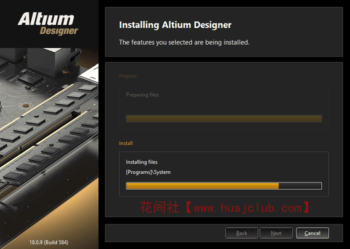
1. After installing the main program, uncheck it and click finish to finish!Ps: Some users' computers will automatically install Microsoft NET4.6.1 according to the configuration requirements. After installation, restart the computer or the installation completion interface as shown in the figure will appear, indicating that the installation is successful.
2. Open the AD20 Crack harmonic file, copy and paste the shfolder.dll file into the installation directory. The default path is C: Program Files Altium AD20. It is recommended to close the antivirus software when copying
3. Find the "X2.exe" file, double-click to open the Altium Designer 20 software, click the avatar icon in the upper right corner, select "License Management...", find the Add standalone license file, pop up the dialog box to load the license file, and load the Altium Designer 20.alf file to provide harmonious licenses.If a new PCB or schematic diagram can be created, it indicates that the cracking is successful