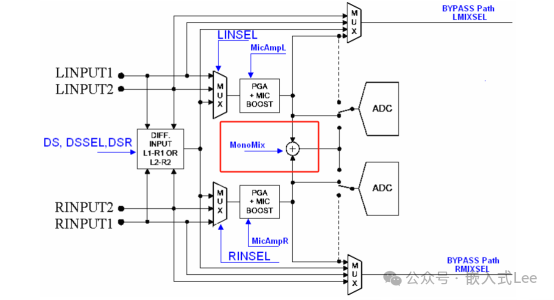
3.6ADC
enter path
The system block diagram is as follows
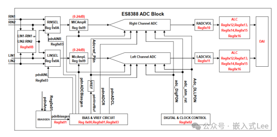


Two channels are supported
,
So there are two
ADC
。
four
Input pins that can be used to support connections to multiple microphones or line input sources..
Two analog inputs
LlNPUT1/2 RlNPUT1/2
It can be selected by the switch and can be used to support the connection with multiple microphones or line input sources. The input multiplexers on the left and right channels can be used to select different configurations for each input source.
Then proceed
PGA
Gain increase. You can select inputs individually, or you can select(
LlNPUT1-RlNPUT1
)Or(
LlNPUT2-RlNPUT2
)The analog input path can support line input or microphone input in single ended mode, pseudo differential mode and full differential mode. These inputs can be configured for microphone or line level. Then, the signal enters high quality
ADC
。 Alternatively, the two channels can also be mixed in the analog domain, and
ADC
While another
ADC
close. On one chip
ALC
The module can be used to control the signal level during recording.
PGA
The gain of can be controlled by the user or on chip
ALC
Function control. In some configurations, the input stage can also provide common mode noise rejection.
The left and right analog input channels are routed to
ADC
, where it is digitized. Alternatively, the two channels can also be mixed in the analog domain, and
ADC
While another
ADC
close. Mono mixed signals appear on two digital output channels.
Each channel also has one
BYPASS
Paths that enable analog input signals to be routed directly to the output multiplexer and
PGA
, without passing
ADC
。
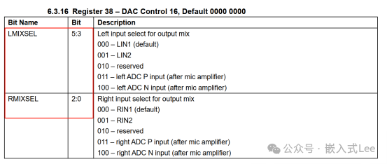
one
Input form
Input Selection
Four input pins
LINPUT1/LINPUT2; RINPUT1/RINPUT2,
Corresponding to two channels
.
Each channel can be selected
one
perhaps
two
perhaps
L-R
Differential pair input
(
Note that the differential pair here is
L-R
no
1-2)
, via selector
MUX
Control, where
(1)
Is bypass mode
(
Pass through output
)
Selection of,
(2)
Yes Enter
ADC
Selection of.
among
(1)
At
MUX
Corresponding register
ten
Of
LINSEL
and
RINSEL
Field control
among
(2)
At
MUX
Corresponding register
thirty-eight
Of
LMIXSEL
and
RMIXSEL
Control.
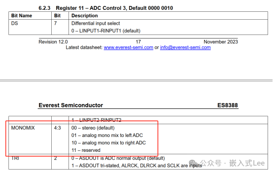
The description of the register here
011
and
one hundred
It seems that it does not correspond to the figure. The figure should be the sum of the difference values
PGA
Value after.
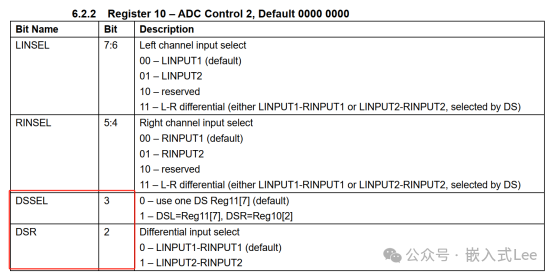
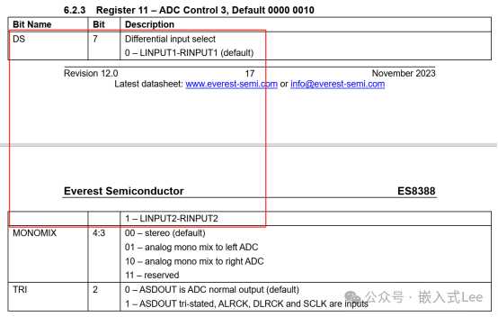
Differential input
The difference is generated by the following parts, which can be
L1-R1/L2-R2
The difference of can also be
R1-L1/R2-R1
Difference of
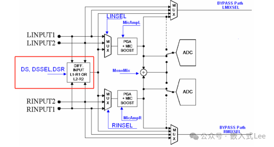
Via register
ten
And register
eleven
Control. If register
ten
Of
DSSEL
by
zero
be
L
and
R
Both use registers
ten
Of
DSR
control
;
If register
ten
Of
DSSEL
by
1,
be
L
Use register
eleven
Of
DS
control
; R
Use register
ten
Of
DSR
Control.
The latter is more flexible, that is
L
and
R
It can be controlled separately.
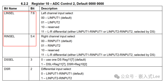
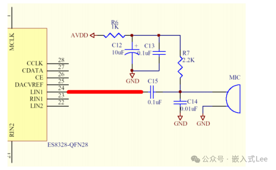
Input schematic
Single ended input
When register ten In
Linsel
and
Rinsel
Not set to
“11”
When,
ES8388
Apply to single ended microphone input mode. Single microphone input signal can be connected to
LIN1
、
RIN1
、
LIN2
or
RIN2
。
Micampl
or
Micampr
It can be used to improve the microphone signal level. Single ended microphone mode cannot provide general mode noise suppression
, as shown below, the input level uses
R7
Pull up offset is performed.
Pseudo differential input
When register ten In
Linsel
and
Rinsel
Set to
“11”
When,
ES8388
Apply to pseudo differential microphone input mode. The pseudo differential microphone input signal can be connected to the
LIN1
and
RIN1
or
LIN2
and
RIN2
。
micampl
and
micampr
It can be used to improve the microphone signal level. When
GND
Pseudo differential microphone mode can provide common mode noise suppression when there is obvious noise
Can be configured as
L-R
still
R-L
, the difference from single end is
GND
Input can be reduced
GND
Common mode noise.
Differential mode
When register ten In
Linsel
and
Rinsel
Set to
“11”
When,
ES8388
Apply to full differential microphone input mode. The fully differential microphone input signal can be connected to the
LIN1
and
RIN1
or
LIN2
and
RIN2
。
micampl
and
micampr
It can be used to improve the microphone signal level. The fully differential microphone mode can provide general mode noise suppression. The recording capacity in full differential mode shall be that in pseudo differential mode
two
Times. It is recommended to use the fully differential microphone mode to record the microphone.
The difference with pseudo differential is that the other end is not connected
GND
It is directly connected to the input signal.

two
bypass mode
INPUT1
perhaps
INPUT2
perhaps
LR
The above signals are directly or through
PGA
After that, you can use the
MUX
Direct output to
DAC
。 I.e
one
About
(1)
At
MUX
Description of.
LMIXSEL and
RMIXSEL
The control bit is used to select the input channel of the left and right bypass paths. The selected input channel can be routed directly to the output multiplexer and
PGA
。
three
gain
It is divided into two parts, one part is simulated
PGA
gain
As shown in the figure below
By register
nine
control
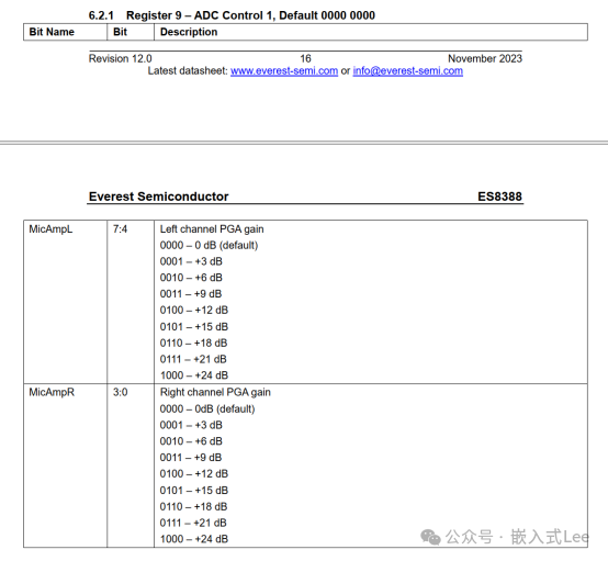
MicAmpL
and
MicAmpR
Control bits are used to control
PGA
To amplify the amplitude of the input signal. The input signal is generated by
LINSEL
and
RINSEL
Control bit selection
Single ended or differential input
。
PGA
Gain can be
0dB
reach
+24dB
Between
3dB
Adjust for step size.
The other part is
ADC
Volume control for
ES8388 ADC The digital volume of can be
-96dB
reach
0dB
Between
0.5dB
To adjust.
RADCVOL
and
RADCVOL
Used to control left and right independently
ADC
Record the volume. If register
fifteen
In
ADCLeR
The control bit is set to
“1”
, you can adjust the left
ADC
Volume to adjust left synchronously
ADC
And right
ADC
The volume of.
four
mute control
register
fifteen
Of
ADCMute Set to
“1”
Mute.
five
mono mix
As shown in the figure below, two channels can be input
MIX
To one
ADC
That is, two channels become one channel.
This is
Mix in analog domain
Of
, and in a ADC While another
ADC
close. By setting
MONOMIX
Set to
“01”
or
“10”
, you can route mono mixed signals to the left
ADC
Or right
ADC
。 For analog mono mixing, you can use the left or right side
ADC
To close unused
ADC
。 Users can also flexibly use
DATSEL
Control bit selects data of audio interface
How to output to
ASDOUT
upper
。
By register
eleven
Of
MONOMIX
control
six
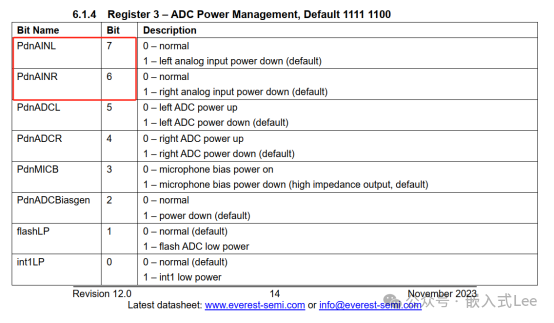
Power on control
By register
three
Of
PdnAINL
and
PdnAINR
Control.
seven
Input reversal control
register fourteen In
ADC_invL
The control bit is used to reverse the left channel
ADC
Polarity.
ADC_invR
The control bit is used for the right channel
ADC
Polarity reversal control of.
eight
High pass filter
register fourteen In
ADC_
H
PF_L and
ADC_
HPF_R
Used to control the left and right
ADC
High pass filtering of
。 It is recommended to set the default setting to ADC_HF_L and
ADC_HF_R
Enable
。
nine
Fade in and out
ADCSoftRamp Control bits for fading in and out
Enable control
。 ADCRampRate The control bit is used to set the soft ramp rate.
The so-called fade in and fade out is to avoid sudden changes and make a certain slope gentle.
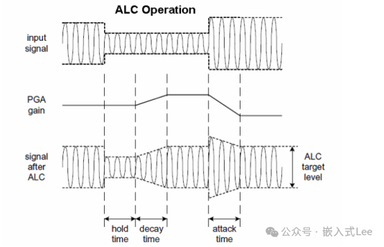
10.ALC
Automatic level control
ES8388 Can be accessed via
I2S/PCM
Interface provides stereo
ADC
Record. Digital output data in
ASDOUT
Send on pin.
ADC
Full scale input level vs
AVDD
Proportional. stay
3.3V
Full scale level is
1.0Vrms
。 Any voltage greater than full scale may cause
ADC
Overload and cause distortion.
ALC
Can proceed
automatic
level
Control. ALC
relevant
Register in register eighteen To register
twenty-two
between
.
When recording
, usually
If you want the volume to remain constant, you can use
ALC Keep the recorded signal at a constant level. For example, when recording sound, the signal may vary greatly, depending on how loud the user's voice is or how close the microphone is to the mouth. This will make the recorded signal hard to hear during playback.
ALC The purpose of the is to maintain a constant output volume regardless of the input signal level. This is achieved by continuously
adjustment PGA Gain
ADC
The signal level at the output remains constant
To achieve
。
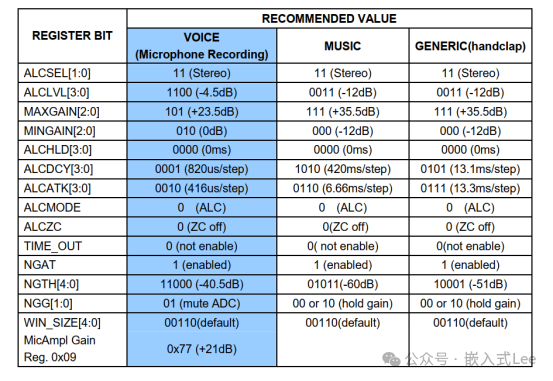
take ALC Setting it to be optimal for each recording source (such as sound, classical music, pop music, etc.) is a rather complicated process. Recommended settings have been provided as the basis for work. The resulting effect is very subjective and may vary from application to application. Some further modifications may be required to optimize the functionality of a particular application, but in most cases, the recommended settings should provide an appropriate solution.
Relevant registers are as follows
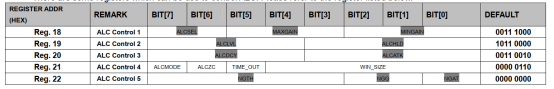
ALC
Related parameters
ALC Enable / ALC Level.
Automatic Level Control Enable / Automatic level control level.
ALC
Function by setting register field
ALCSEL
To enable.
ALCSEL=2'b00:ALC
close;
ALCSEL=2'b01:ALC
Right channel enabled;
ALCSEL=2'b10:ALC
Left channel enabled;
ALCSEL=2'b11:ALC
Enabled. When enabled, you can use the
ALCLVL
Register field pair
ALC
Output volume for programming.
ALC
The level range is
0dBFS
and
-16.5dBFS
Variation between, each stage
1.5dBFS
。 The maximum target level is always not higher than
ADC
Full scale level to help reduce the possibility of clipping signals. This level should be set as high as possible to achieve the best SNR performance, but not too high to allow signal clipping when the signal changes. The more unstable the signal level is,
ALC
Target level and
ADC
The greater the clearance required between full-scale levels.
ALC Maximum Gain.
ALC Maximum gain. By setting register fields
MAXGAIN
To impose
PGA
The upper limit of the gain.
MAXGAIN
The range of
-6.5dBFS
and
35.5dBFS
Change between, each step
6dBFS
。 The purpose of maximum gain is to ensure that small input signals are
ALC
It is contained by the function and will not be over magnified. The recorded music track fades out; For example, if the recorded music track fades out;
“
Maximum gain
”
Set Prevention
ALC
Destroy the effect by increasing the gain when the music signal decays. The maximum gain shall be determined according to the level of the quiet signal that shall be regarded as the fading signal determined by the designer.
ALC Minimum Gain.
ALC Minimum gain. By setting register fields
MINGAIN
To impose
PGA
The lower limit of the gain.
MINGAIN
The range of
-12dBFS
and
30dBFS
Change between, each step
6dBFS
。 The purpose of minimum gain is to ensure that large input signals are allowed and will not be
ALC
The function is excessively attenuated. If the minimum gain is large, then
ALC
The ability to control the signal level will be limited, and it is more likely that it cannot prevent large signal distortion. However, if the minimum gain is small, a larger attenuation will be applied to the large signal, which may unnecessarily limit the dynamic range of the processed signal. The minimum gain should be set as low as possible, certainly not greater than the maximum input signal adjusted downward to
ALC
Gain required for the target level.
ALC Hold Time
Hold time. Detect the signal level lower than the target level and PGA The time delay between the start of gain rise is determined by
field ALCHLD 。 It can be set to zero or
two
Power
(2n)
Step programming, e.g
2.67ms, 5.33ms, 10.67ms
Wait until
1.36s
。
Please note that, ALC Hold time applies only to gain increments
;
When the signal level is higher than, there is no delay before reducing the gain
Objectives. ALC Hold time inactive in limiter mode
(
See below
)
。
The purpose of this delay is to ensure that
ALC
Will not overreact to changing signal levels. Should be as required
ALC
The type of response sets the hold time. If it is necessary to adjust the gain of the changed signal immediately, a short holding time shall be used;
This may apply to voice applications. If you want to proceed more carefully
ALC
For gain adjustment, a longer holding time should be used to respond only to long-term signal level changes and maintain the original signal dynamics to a greater extent; This may apply to music with a large dynamic range, as is often found in classical music.
ALC Decay Time.
ALC
Attenuation time.
ALC
rise
PGA
The time taken for gain is determined by the register field
ALCDCY
Control.
ALC
The decay time is defined as the time of each gain step. It can be pressed twice(
2n
)The power of step is used for programming, such as
410us/
Step
820us/
Step and
1.64ms/
Step, up to
420ms/
Step. Attenuation time determination
ALC
Speed of adjustment in response to signal level drop. If rapid response to changing signals is required, a shorter decay time should be used. The attenuation time shall not be short enough to cause
ALC
Fast response to nominal constant signal level. For example, if the input signal may have a pause or mute, the decay time should be set long enough to ensure that
ALC
During these durations, no major gain adjustments are made.
ALC Attack Time.
ALC
Attack time.
ALC
Slope descent
PGA
The time taken for gain is determined by the register field
ALCATK
Control.
ALC
The attack time is defined as the time of each gain step. It can take two(
2n
)To the power of steps, such as
104us/
Step length
208us/
Step size and
416us/
Step length, etc., up to
106ms/6dB
。 Its measurement is similar to the decay time. The advantage of short attack time is that it can respond quickly to the increased signal level. This in turn reduces the possibility of shearing. Many of the same considerations as Hold Time and Falloff Time also apply. The attack time should be set together with the decay time. If the system needs fast response, such as voice application, it may need faster attack
/
Time of decline. On the other hand, slower attacks if more stable input signals are expected
/
The recession time may be the most appropriate.
ALC Mode.
ALC
pattern. Two operation modes can be realized through register bit
ALCMODE
use. By setting
ALCMODE=0
To select normal
ALC
Operation. By setting
ALCMODE=1
To select the limit mode. In restricted mode,
ALC
The maximum gain is set equal to
PGA
set up. In this mode, the signal level can be reduced to prevent overload, but cannot be increased to the initial level
PGA
Gain setting above - register field is not used when limiter mode is selected
MAXGAIN
。 In limiter mode, the operation speed of the gain control circuit is approximately fast
four
Times to allow rapid reduction of high signal level and rapid increase of low signal level. Do not use limiter mode during microphone recording.
Peak Limiter.
Peak limiter. To avoid
PGA
Clipping when a large signal is applied just after the gain rises for a period of time (for example, after a quiet period of time),
ALC
The circuit includes a peak limiter function. If
PGA
The input signal after the gain exceeds the peak threshold (fixed below full scale
1.5dB
), then
PGA
Gain declines at maximum attack rate (e.g
ALCATK
=
0000
Until the signal level drops below the peak threshold. This function is always enabled whenever automatic level control is enabled.
Sample Rate.
Sampling rate.
ALC
The hold, decay, and attack times will vary slightly depending on the sampling rate used. For example, when
48kHz
When sampling,
ALC
The hold, decay, and attack times are equal to the values in the register definitions. If the actual sampling rate is
44.1kHz
, then
ALC
Holding, attenuation and attack time will be reduced proportionally
44.1/48
。
ALC Zero Cross/Time out.
ALC
Zero crossing
/
Timeout. Register field
ALCZC
For control
PGA
Whether the gain update is timed to occur at the zero crossing point of the input signal. Enabling this feature ensures that the
PGA
Pop up and click caused by gain adjustment, but this function may also cause faster
ALC
Response. If
PGA
If the gain step is small enough to eliminate the need for zero crossing detection, the zero crossing option is not required. A timeout is provided to ensure that if zero crossing does not occur within a fixed time, the gain can still be updated. Timeout is set through register
TIME_OUT
Enabled. It is not automatically enabled.
Noise Gate Enable / Noise Gate Threshold / Noise Gate Type.
Noise Gate Enable
/
Noise gate threshold
/
Type of noise gate. The noise gate function sets the register field
NGAT
To enable. When enabled, you can use the
NGTH
The register field programs the noise gate threshold. The range of noise gate threshold is
-76.5dBFS
and
-30dBFS
Change between, each step
1.5dBFS
; The threshold is the input signal level, which is lower than the input signal level
PGA
The gain will be muted or kept constant. You can use the register field
NGG
Set the noise gate type (mute or hold gain).
ALC
Reference settings
one
For voice recording, fast ALC Respond so as to quickly compensate the voice of different people and the movement relative to the microphone
。
two
For music recording, fast response is not recommended because it may cause clipping in response to any sudden change in the level of the music signal. Decreasing the maximum gain setting can help avoid clipping when the music level increases after a quiet period, and limit ALC The degree of adjustment. This may not be what all music applications want, so it is not shown in the recommended settings. This is one of many adjustments that users should consider when optimizing for a known operating environment.
three
For general recording,
ALC
You must try to accommodate all types of sound, and you must find a compromise setting. For those who can tolerate the pulse of applause
ALC
Response, therefore, it is recommended that
ALC
The attack time should not be set too fast,
ALC
The attenuation time should not be set too slowly. If necessary, adjust the minimum and maximum gain settings to limit
ALC
Range of control. The combination of settings should allow
ALC
Fast response to signal level changes and pulse type sound, but also minimize the gain pump caused by related level changes.