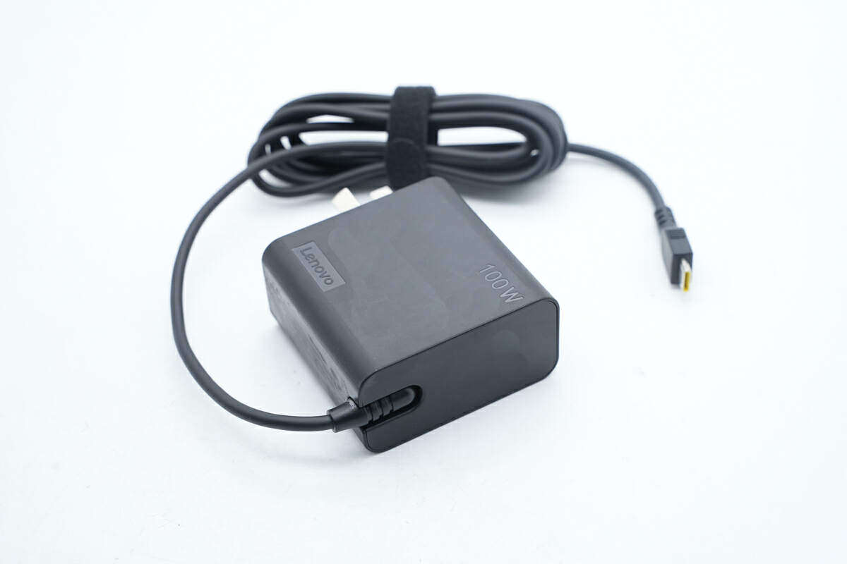
I got the charging head networkassociationOriginal of new laptop100WGallium nitridePower adapter, this adapter is designed with its own cable, and the length of the output cable is about 1.8 meters.The charger supports 100-240Vac wide voltage input, 20V5A PD fast charging, and 5-21V3A PPS fast charging. It is also compatible with mobile phone charging.
This power adapter is manufactured by Delta and has three national standard pins. It not only has the grounding function, but also the metal shell of the computer will not numb your hands when using, and it is more firm and not easy to fall off.Here comesassociationOriginal100WGallium nitrideTake a look at the internal scheme and materials for disassembly of the power adapter.
associationOriginal100WGallium nitrideThe power adapter is in classic black asassociationThe standard power adapter of its notebook benefits fromGallium nitrideWith the adoption of technology, the overall design of the fuselage is very small.
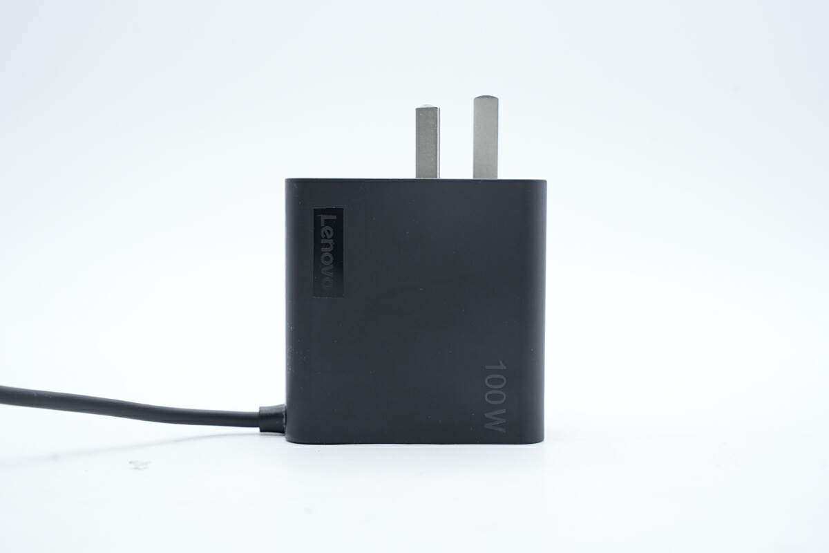
The adapter adopts PC flame-retardant plastic shell, the main body is frosted and fingerprint resistant, the height and width of the machine are the same, and the front view is square.
The front of the fuselage is designed with the Lenovo brand.
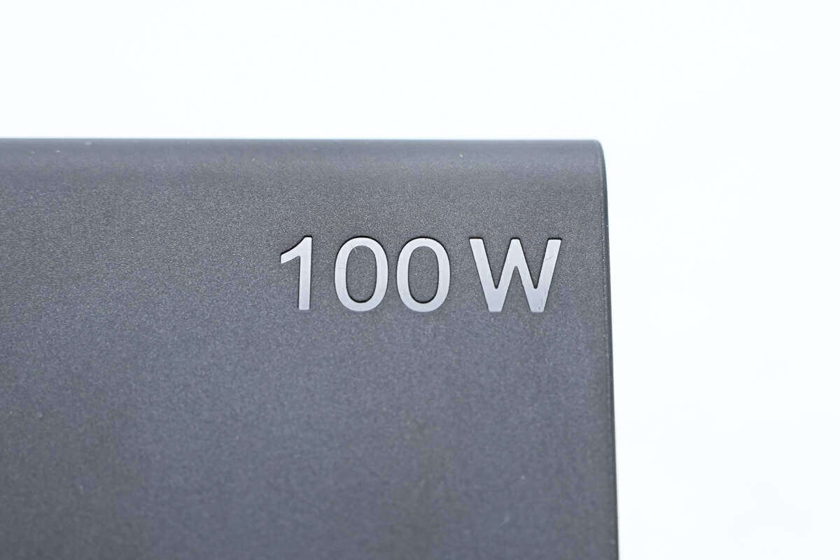
The diagonal is designed with100WWords, users can intuitively understand the maximum output power of this power adapter.
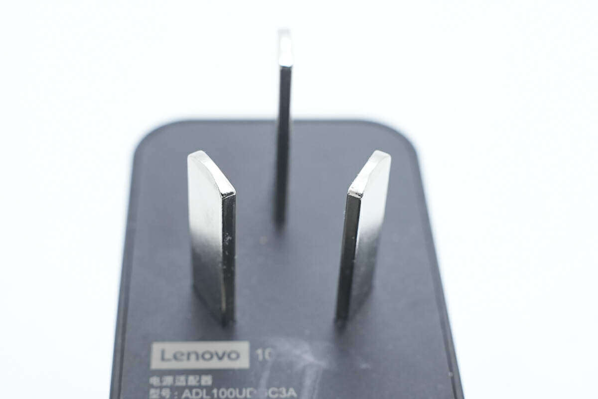
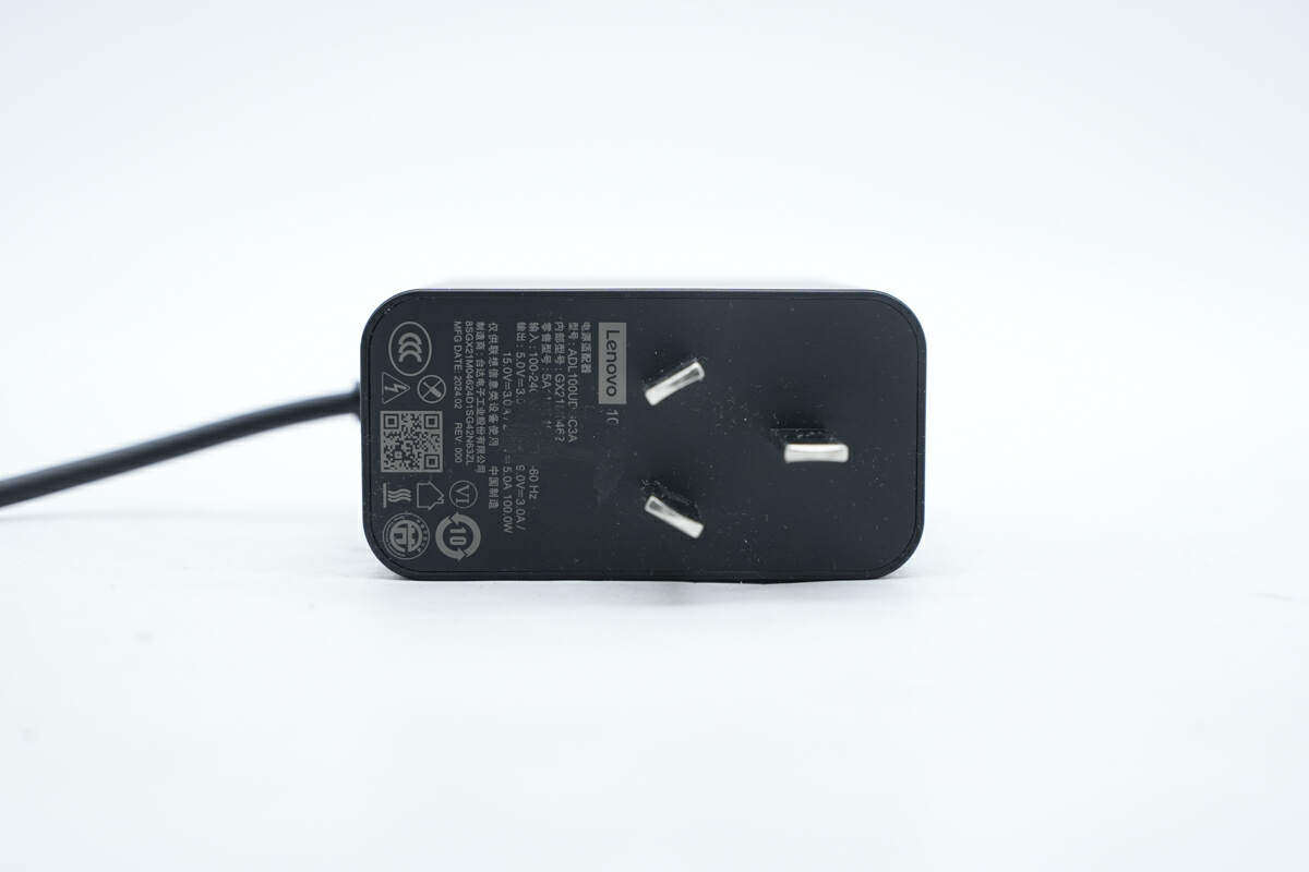
The power adapter is equipped with three pin pins, which can be grounded to effectively avoid electric shock and improve the charging experience.
The input housing is printed with power adapter parameter information.
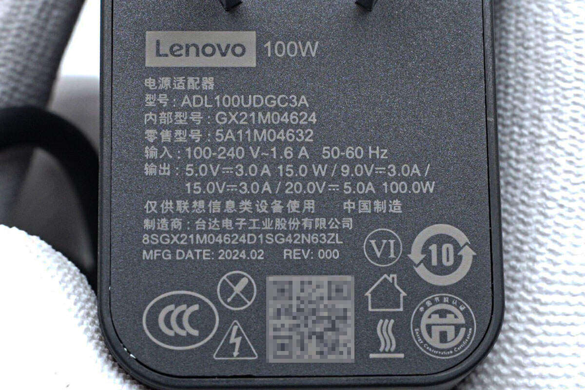
Close up of power adapter nameplate parameters
Model: ADL100UDGC3A
Internal model: GX21M04624
Retail model: 5A11M04632
Input: 100-240V~1.6A 50/60Hz
Output: 5V3A, 9V3A, 15V3A, 20V5A 100W
Manufacturer: Delta Electronics Industry Co., Ltd
The adapter has passed CCC certification and Class VI energy efficiency certification.
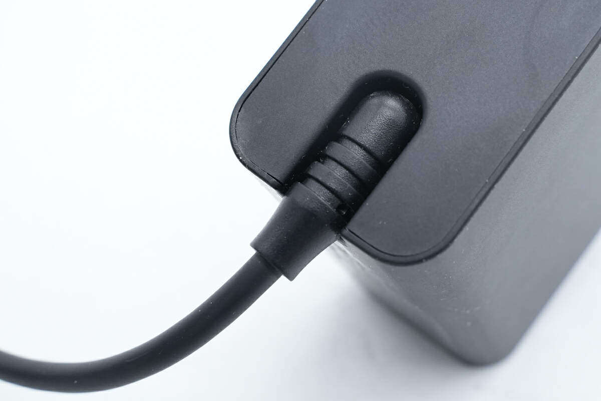
Groove protection design is made at the connection between the output line and the fuselage.
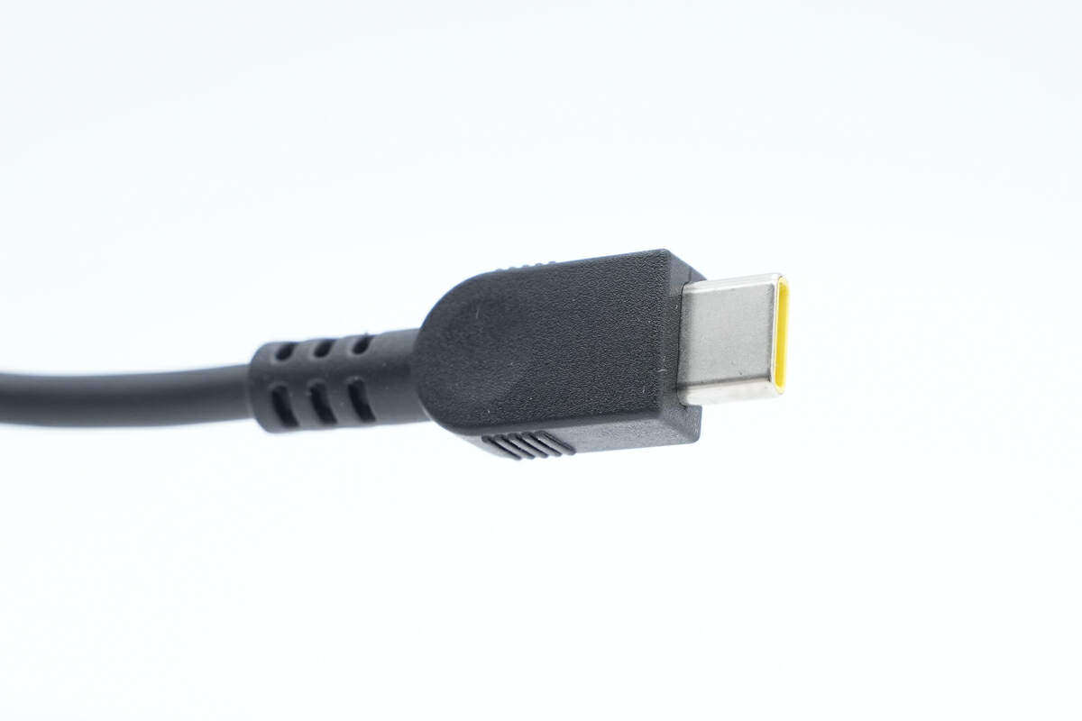
The USB-C terminal housing is sanded, and the front, back and both sides are designed with classic small concave and convex teeth, which is convenient for users to plug in and out.
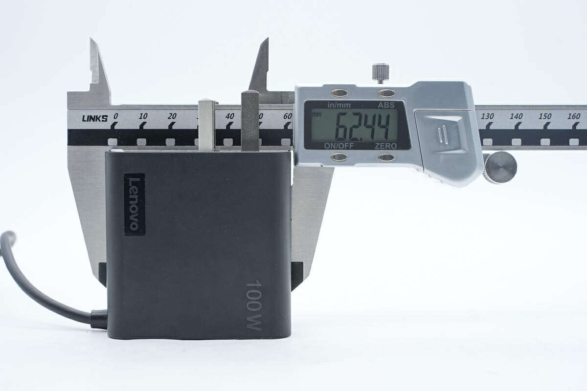
The measured width and height of the power adapter body are about 62.4mm.
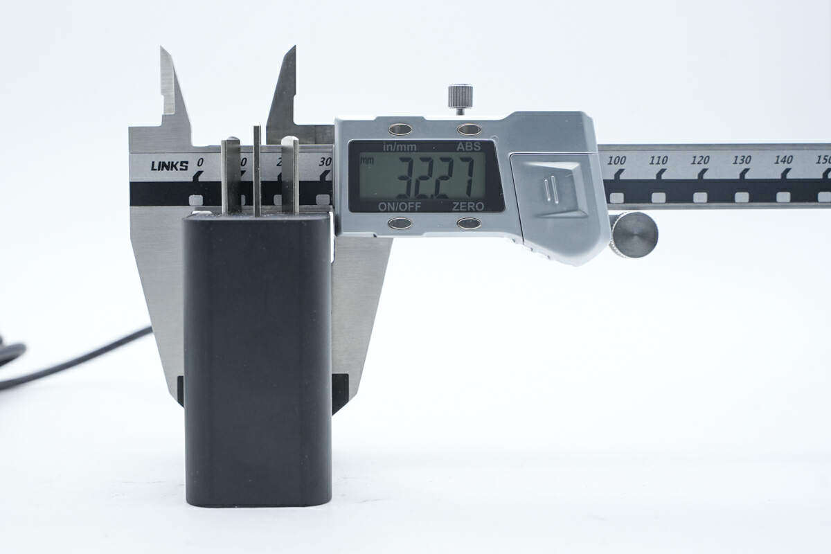
The thickness of the fuselage is 32.27mm.
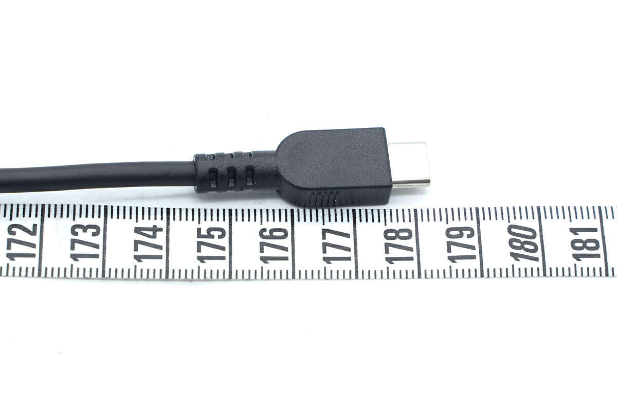
The length of USB-C line is about 178.3mm.
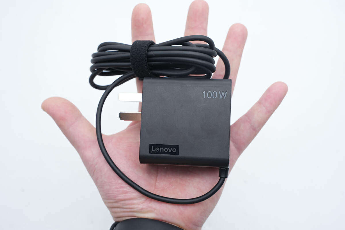
The size of the power adapter in your hand is intuitive.
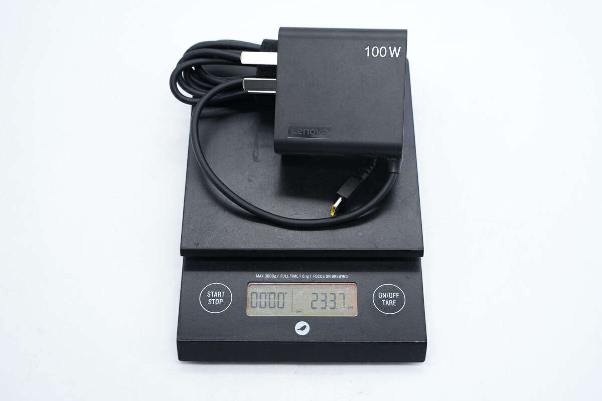
In addition, the measured product weight is about 234g.
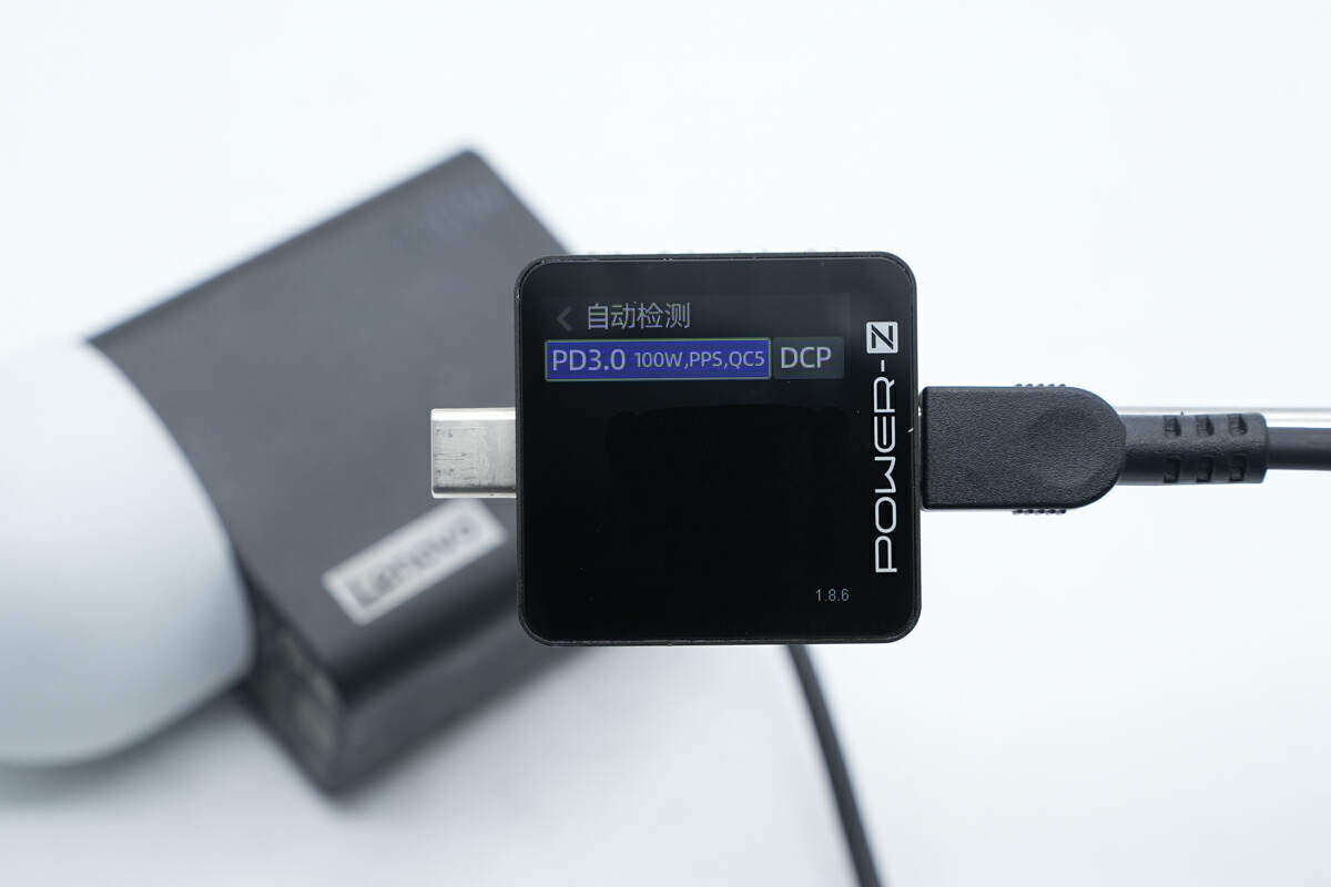
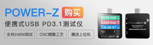
Using ChargeLAB POWER-Z KM003C, it is measured that the USB-C output of the power adapter supports PD3.0, PPS, QC5, and DCP charging protocols.
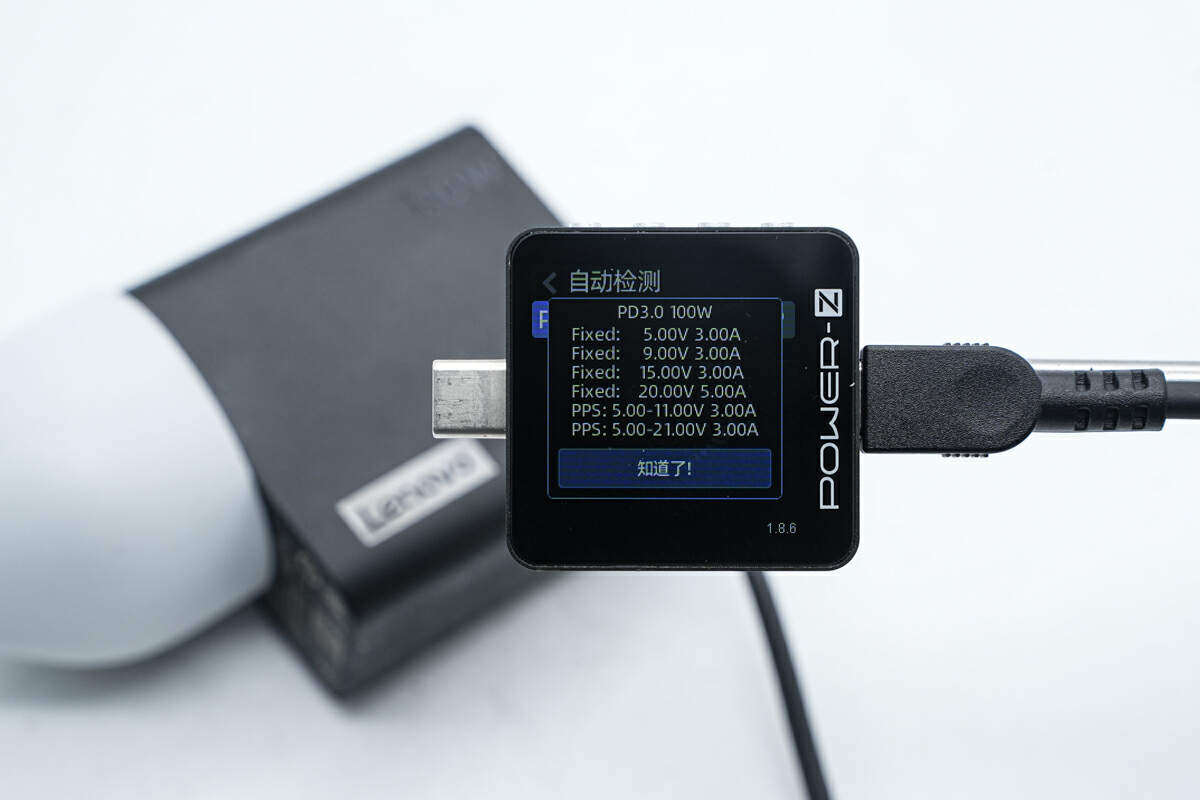
PDO message display also has four groups of fixed voltage gears: 5V3A, 9V3A, 15V3A, 20V5A, and two groups of PPS voltage gears: 5-11V3A, 5-21V3A.
Disassembly of Lenovo original 100W GaN power adapter
After seeing the appearance and test of Lenovo's GaN power adapter, we will disassemble it to see the internal plan and materials.
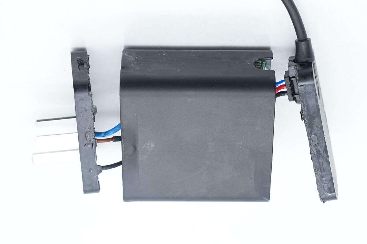
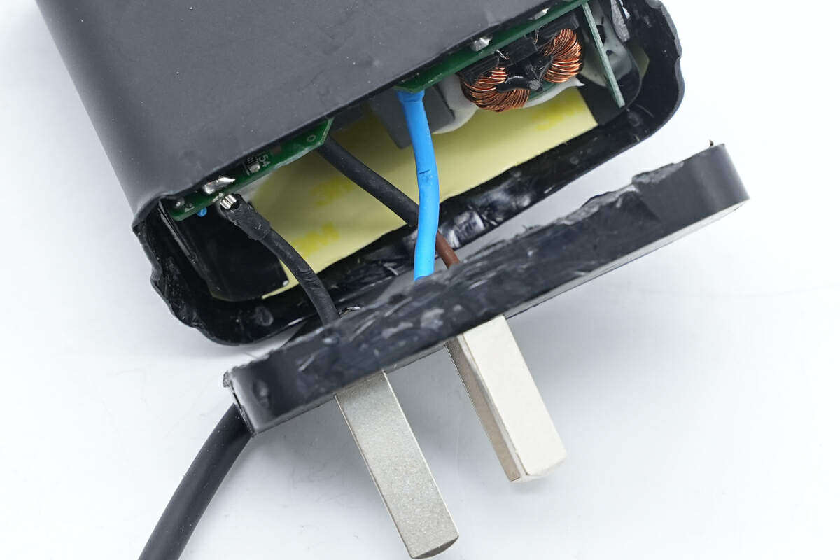
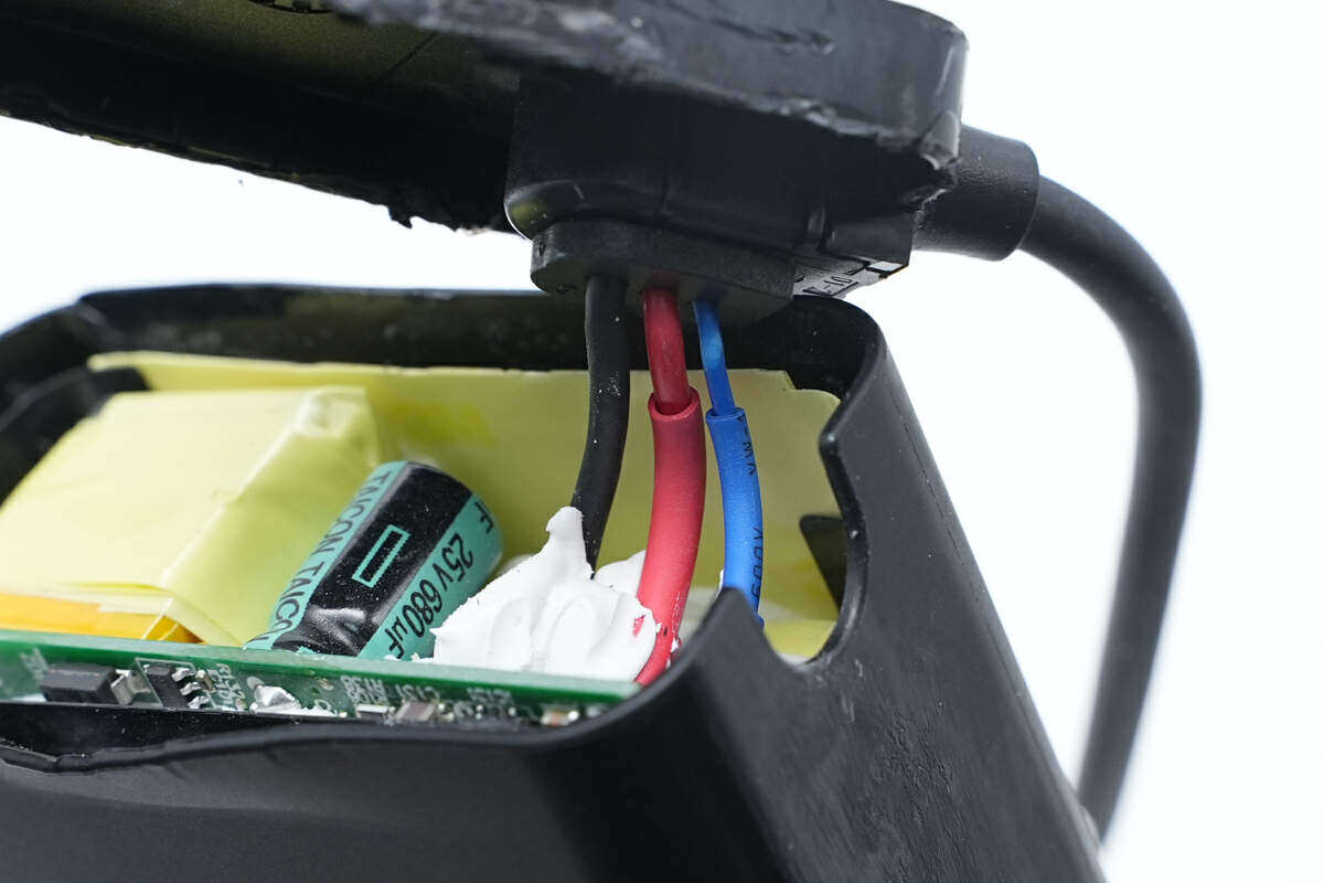
First, disassemble the input and output side housing of the adapter.
The power input wire is connected by welding.
The output end is also connected by wire welding.
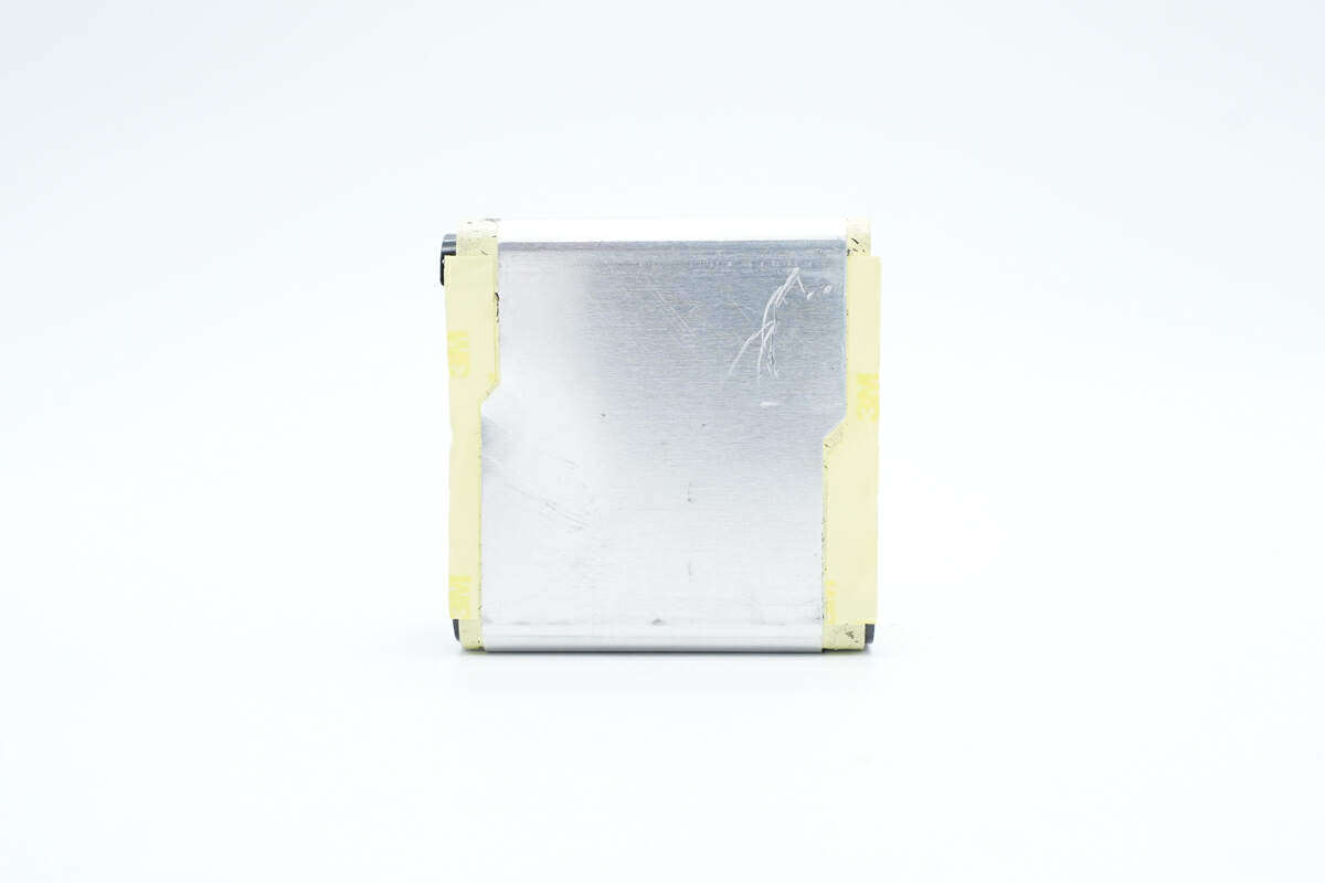
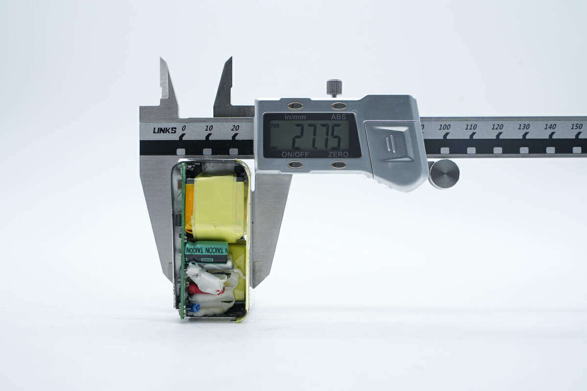
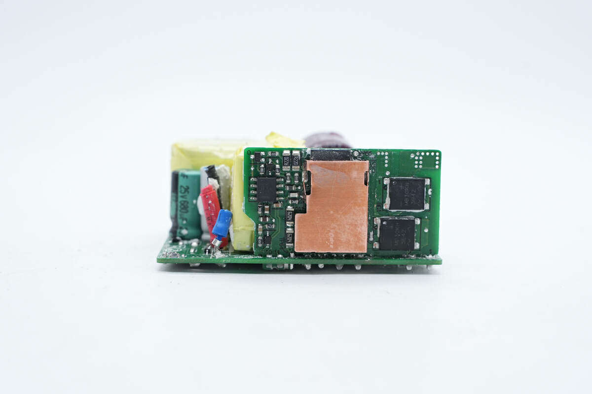
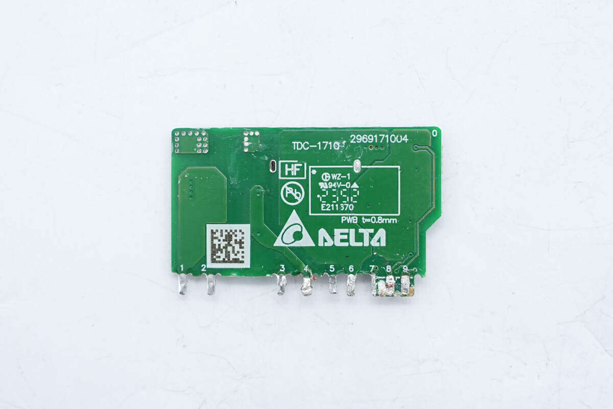
Cut the connecting wire and take out the PCBA module, and the PCBA module is wrapped with aluminum sheet for heat dissipation.
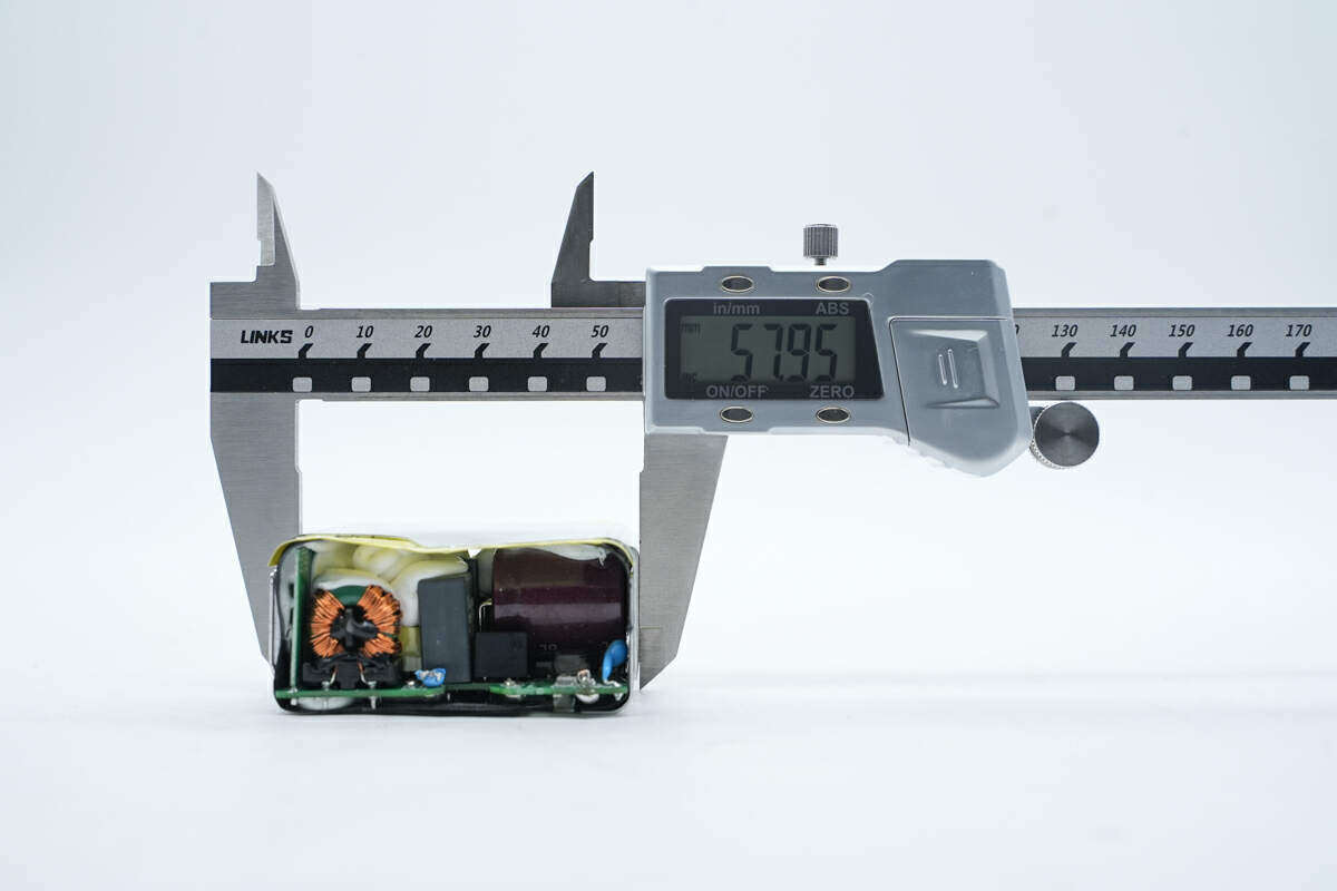
The length of PCBA module measured with vernier caliper is about 57.7mm.
The width of PCBA module is about 58mm.
The thickness of PCBA module is about 27.8mm.
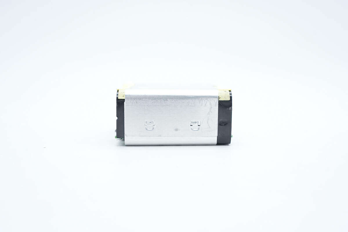
The side of PCBA module is fixed with clips.
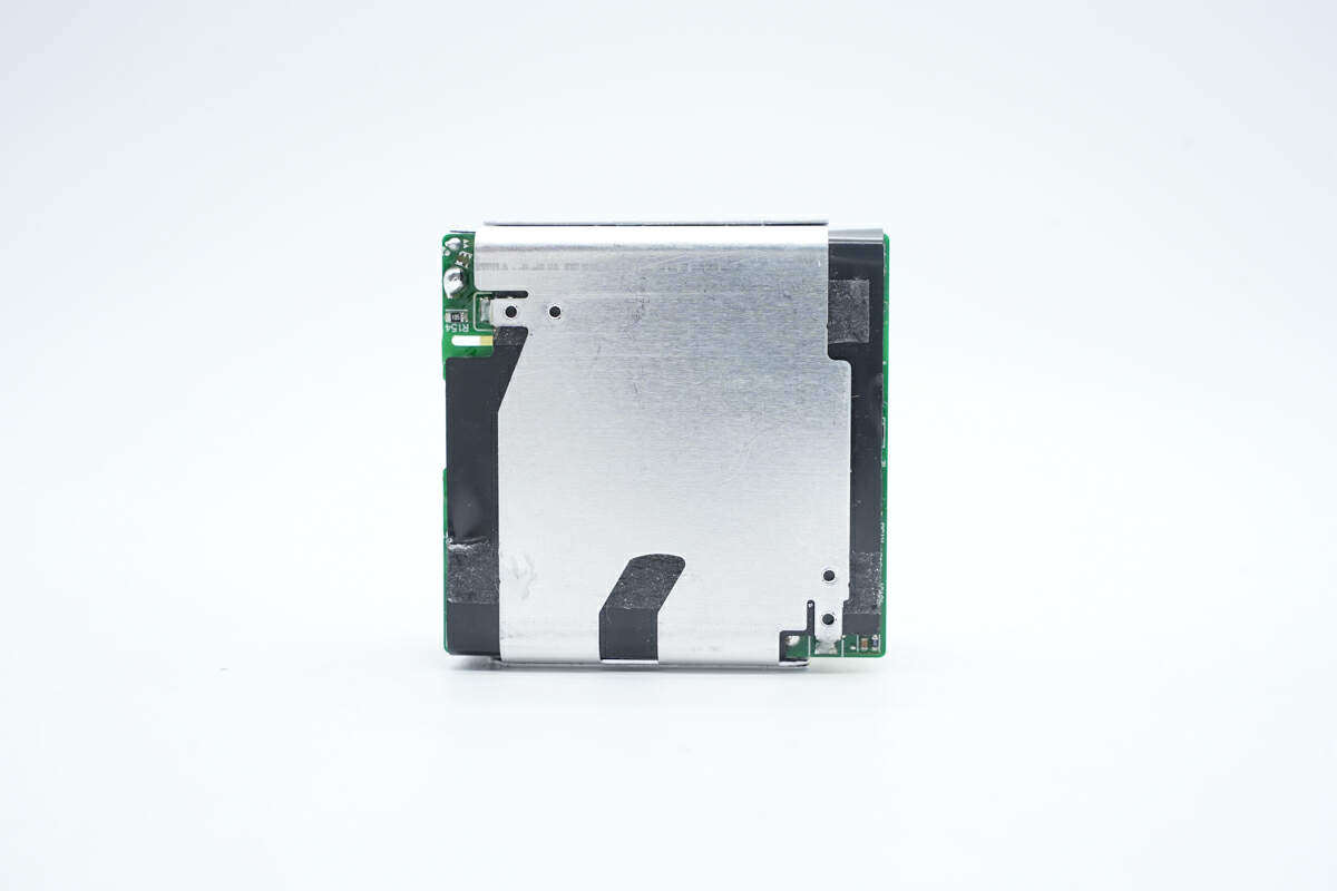
The heat sink riveting solder is welded to the PCBA module.
Close up of heat sink solder joints.
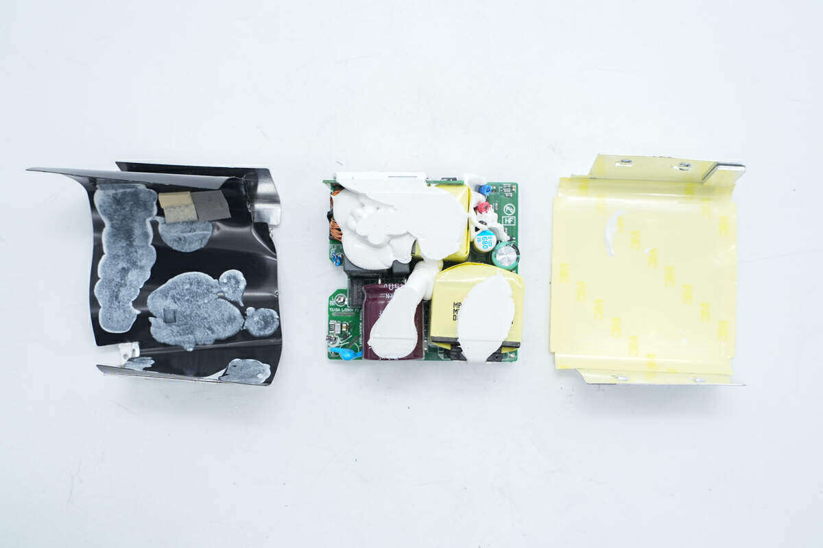
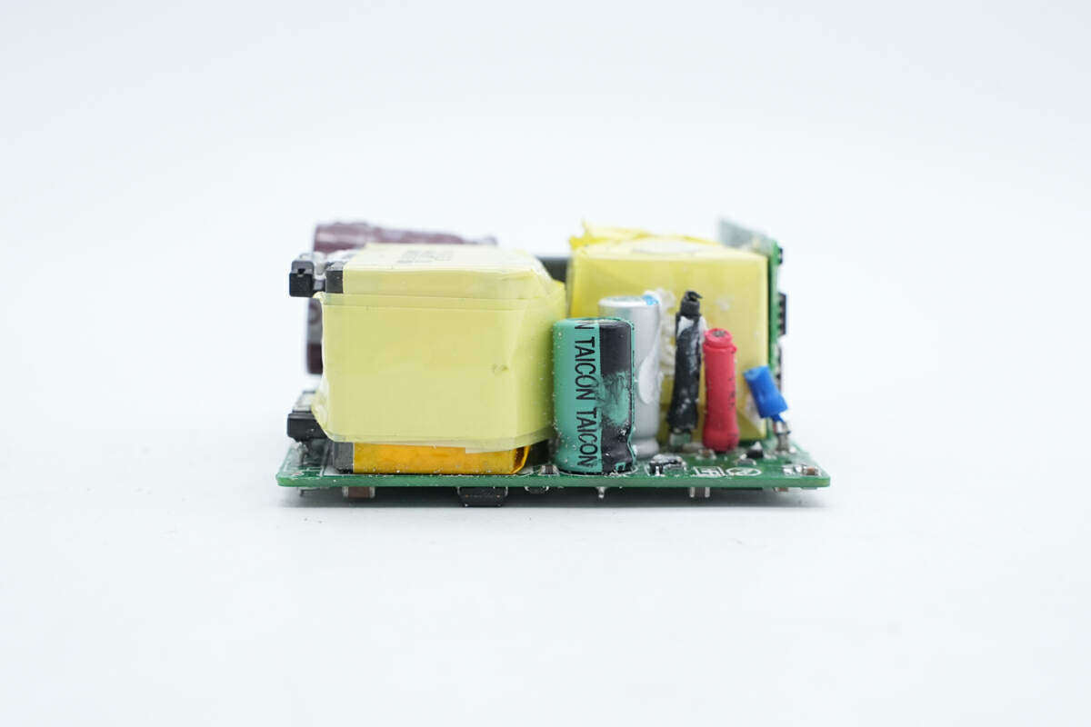
Remove the heat sink wrapped by PCBA module, glue the front and back of PCBA module to strengthen heat dissipation, and set Mylar insulation between the heat sink and PCBA module.
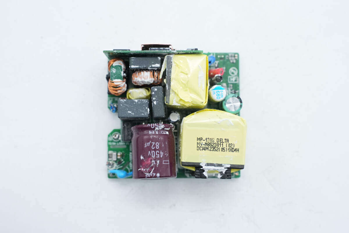
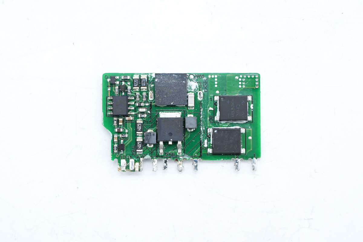
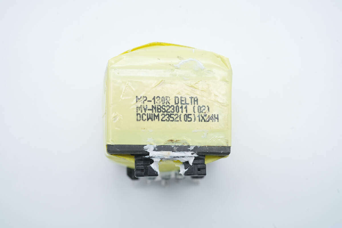
The front of the PCBA module is at a glance, and the left side is equipped with fuse, safety gauge X2 capacitor, and common mode inductance.Weld a small board on the top, which is a rectifier bridge and PFC circuit.The lower part is the PFC boost inductance, and the right side is equipped with an output filter capacitor.The transformer is welded at the lower right corner, and the high-voltage filter capacitor is on the left.
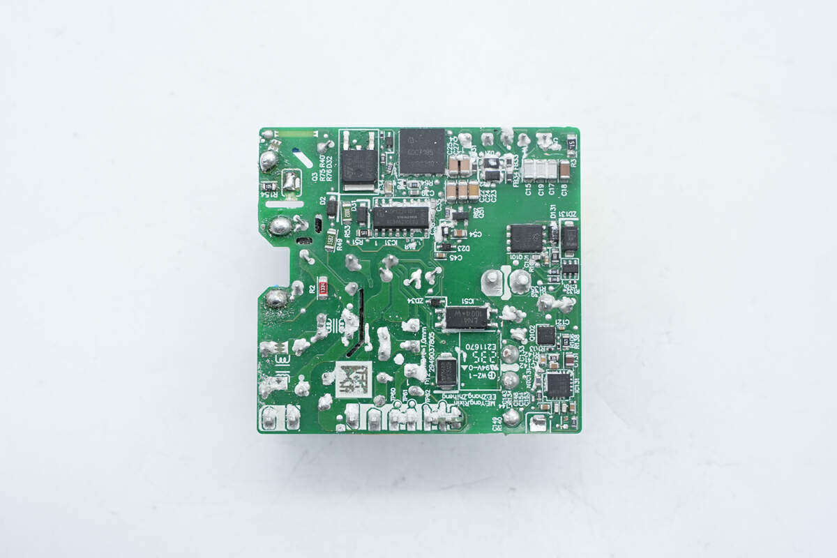
The back of the PCBA module is welded with a hybrid flyback controller and two switch tubes, the lower right corner is welded with a feedback optocoupler, a synchronous rectifier controller, a synchronous rectifier tube and a protocol chip.
Through observation of PCBA module, Lenovo 100W GaN power adapter adopts PFC+HFB hybrid flyback switching power supply architecture, the output voltage is fed back by the protocol chip through optocoupler to achieve wide voltage output, and GaN switches are used at the PFC level.Now let's learn about the design and materials of the entire adapter from the input side.
The input terminal is welded with fuse, safety gauge X2 capacitor and common mode inductance.
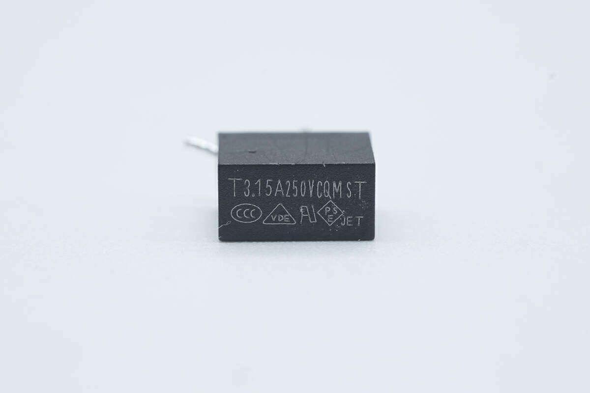
The input fuse is from CONQUER Gongde, MST series ultra small time delay fuse, with the specification of 3.15A 250V, used for input overcurrent protection.
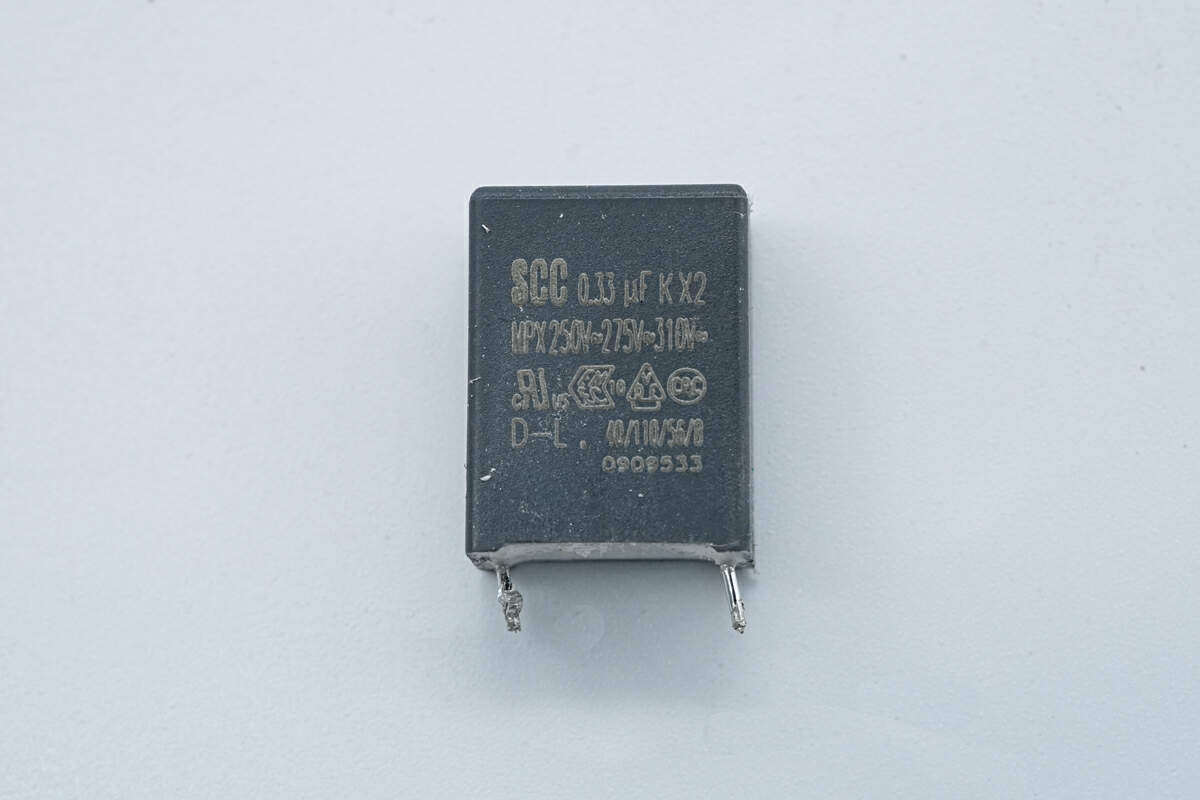
The safety gauge X2 capacitor is from SCC full electronic, and the specification is 0.33 μ F.
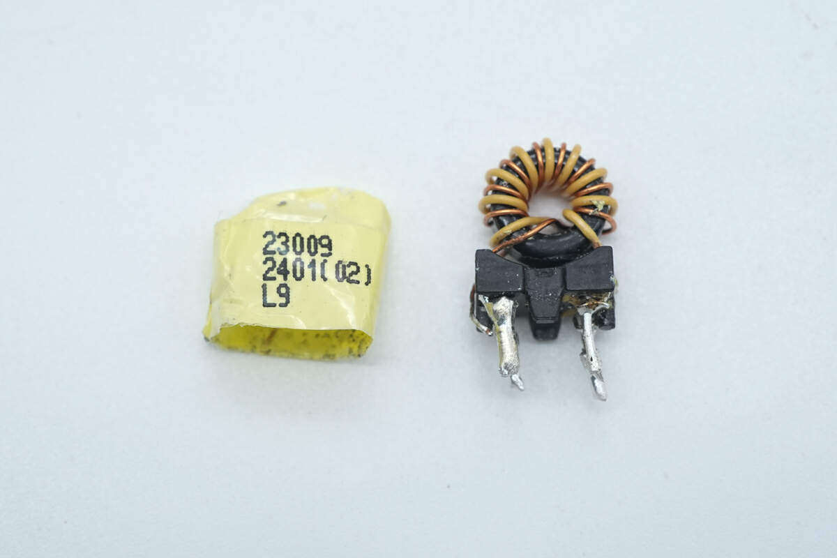
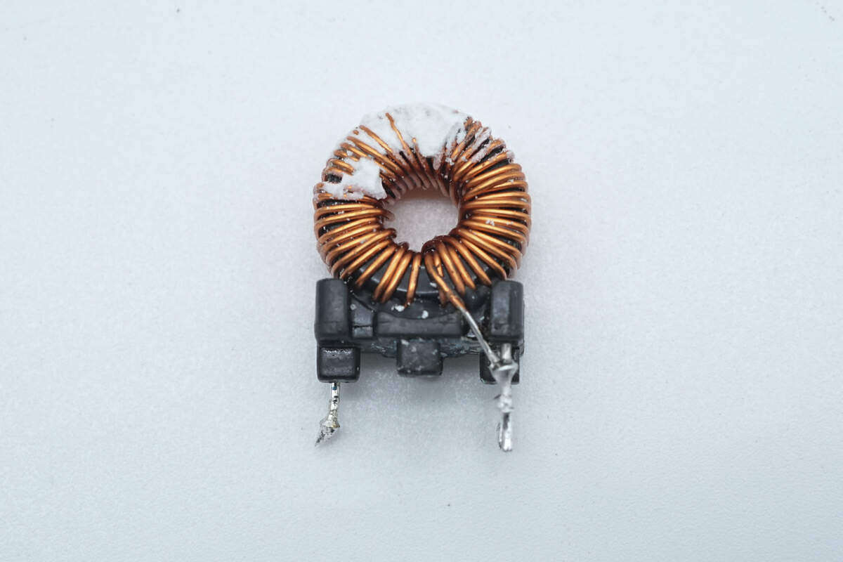
The common mode inductance is wound with enameled wire and insulated wire, with insulated support welded at the bottom and tape wrapped for insulation.
The other common mode inductor is wound with enameled wire, and the insulation support is welded at the bottom.
The small side plate is welded with rectifier bridge, PFC controller, PFC switch tube and PFC rectifier tube.Corresponding switch tube and rectifier tube positions are provided with copper sheets and heat conduction pads to enhance heat dissipation.
Weld and remove the small side plate and the cooling copper fin.
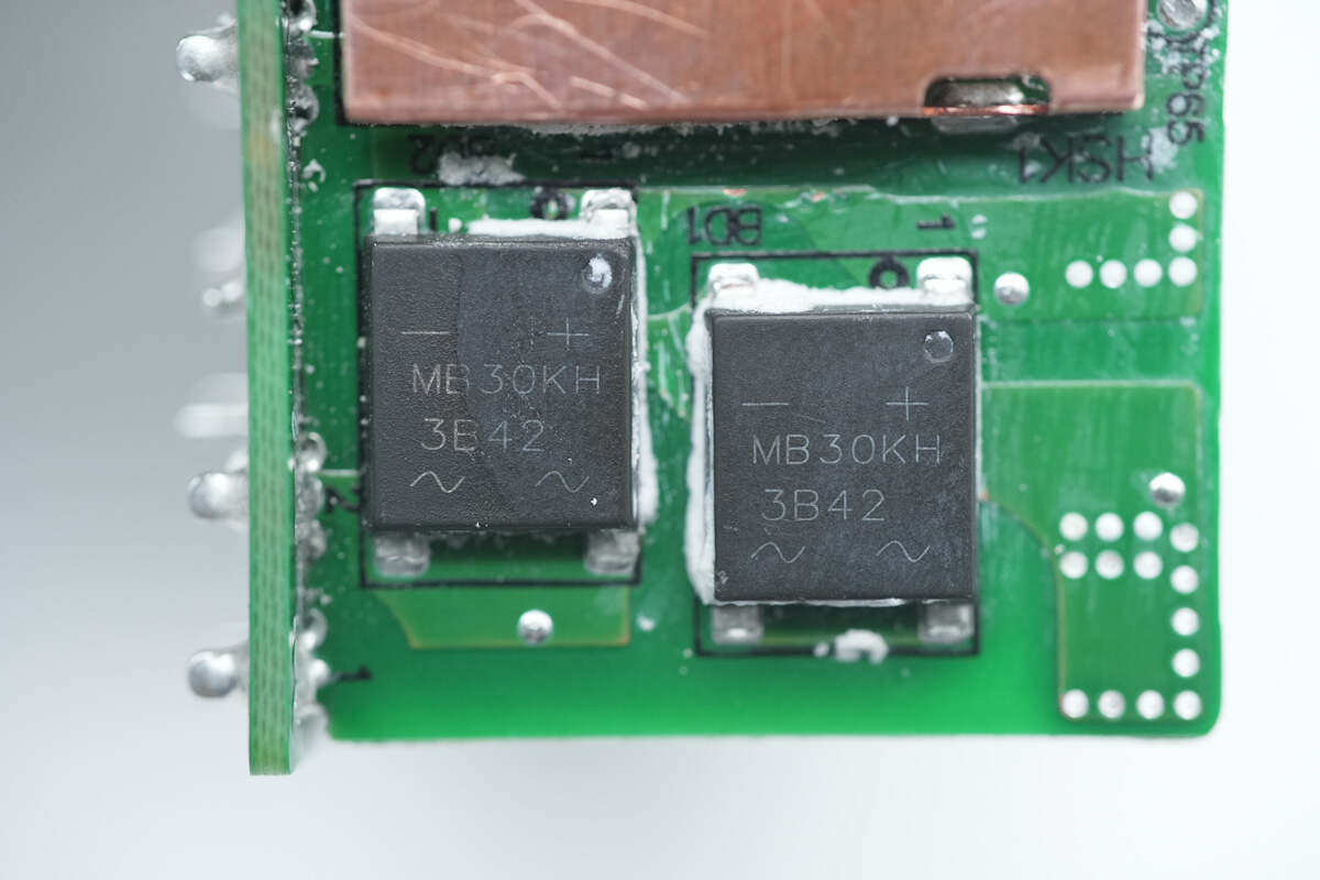
The PFC controller is welded on the left side of the small board, the PFC switch tube is welded on the upper middle part, the rectifier tube is welded on the lower part, and two rectifier bridges are welded on the right side.
There are no welding elements on the back of the small board.
The model of the two rectifier bridges is MB30KH, the specification is 3A1000V, and the half bridge connection is evenly distributed for heating.
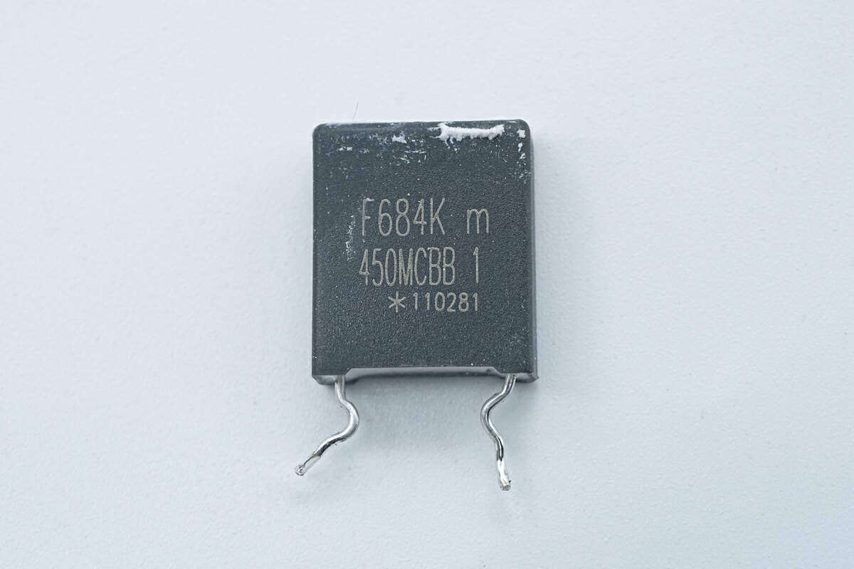
The specification of one film filter capacitor is 0.68 μ F.
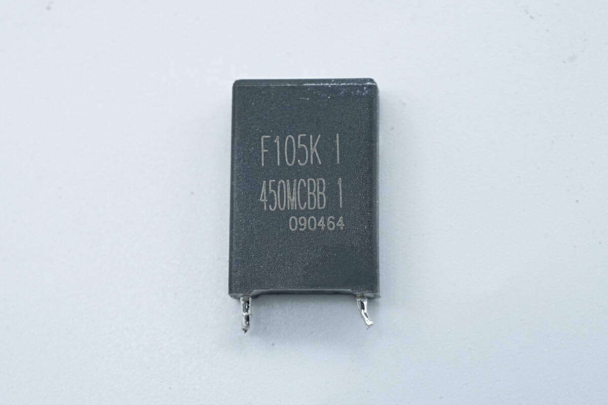
The specification of the other film filter capacitor is 1 μ F.
The filter inductance is wound by magnetic ring, and the insulation support is welded at the bottom.
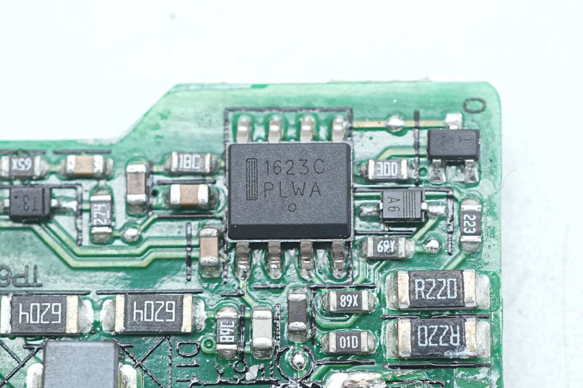
PFC controller is from Ansomy, model NCP1623, which is based on the innovative Valley synchronous frequency turn back (VSFF) method.VSFF can maximize efficiency under nominal load and light load conditions, operate in critical mode under heavy load and intermittent conduction mode under light load, and support valley opening to improve efficiency.
NCP1623 supports critical mode and intermittent conduction mode operation, valley synchronous frequency turn back can improve efficiency under nominal load and light load, and can obtain good power factor under low switching frequency.
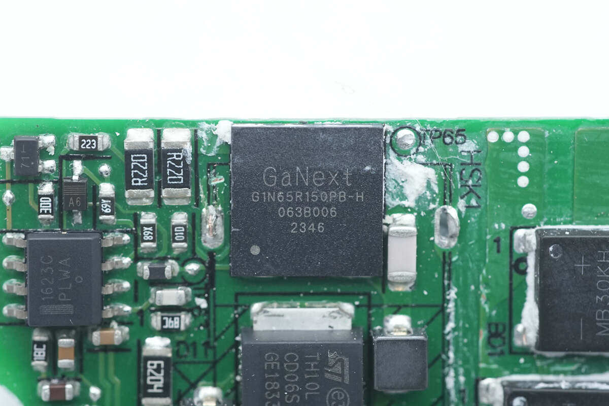
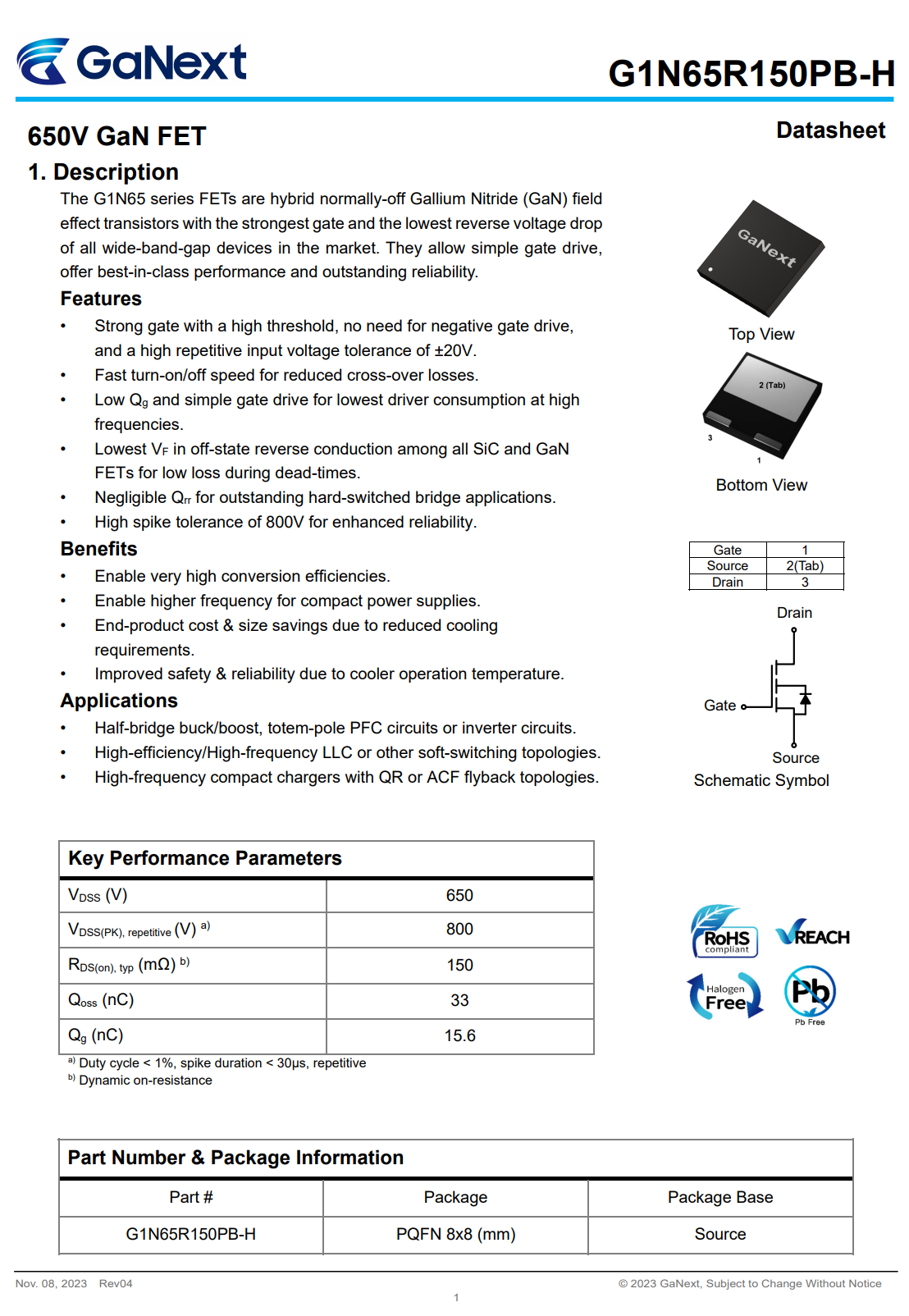
The PFC switch uses Ga Future G1N65R150PB-H, which is a 650V GaN power device. The transient withstand voltage is 800V, the nominal resistance is 150m Ω, and the grid withstand voltage supports ± 20V. The traditional silicon MOS drive can be used. Compared with the enhanced GaN, the design of the grid drive circuit is greatly simplified.
Gallium future G1N65R150PB-H adopts PQFN8x8 packaging, with the heat dissipation pad as the source, reducing the high-frequency wiring area, which helps optimize EMI performance.
The magnetic core of PFC booster inductance is wrapped with copper foil for shielding and pasted with tape for insulation.
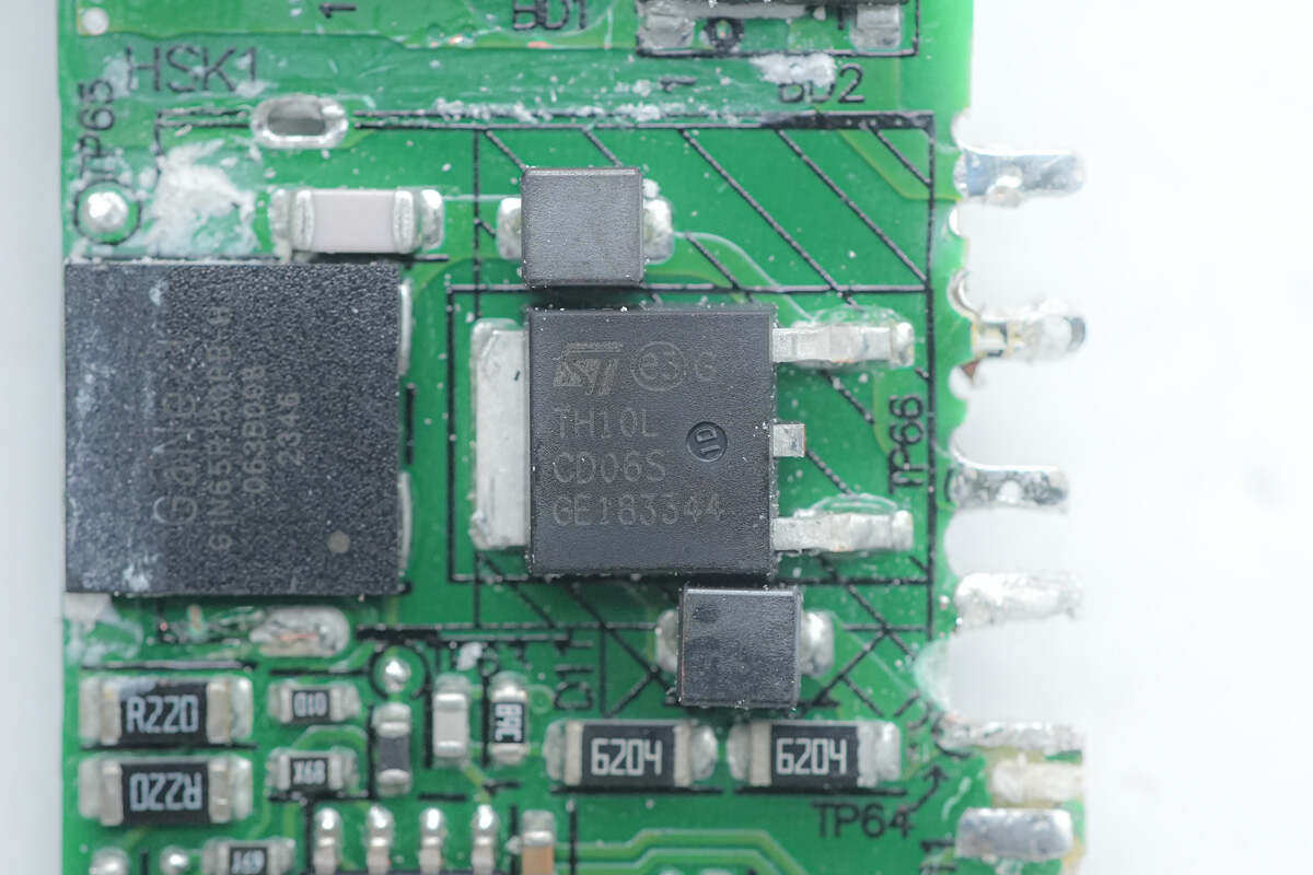
PFC rectifier tube is from ST STTH10LCD06 STTH10LCD06 STTH10LCD06 STTH10LCD06 STTH10LCD06 STTH10LCD06 STTH10LCD06 STTH10LCD06 STTH10LCD06 STTH10LCD06 STTH10LCD06 STTH10LCD06 STTH10LCD06 STTH10LCD06 STTH10LCD06 STTH10LC.
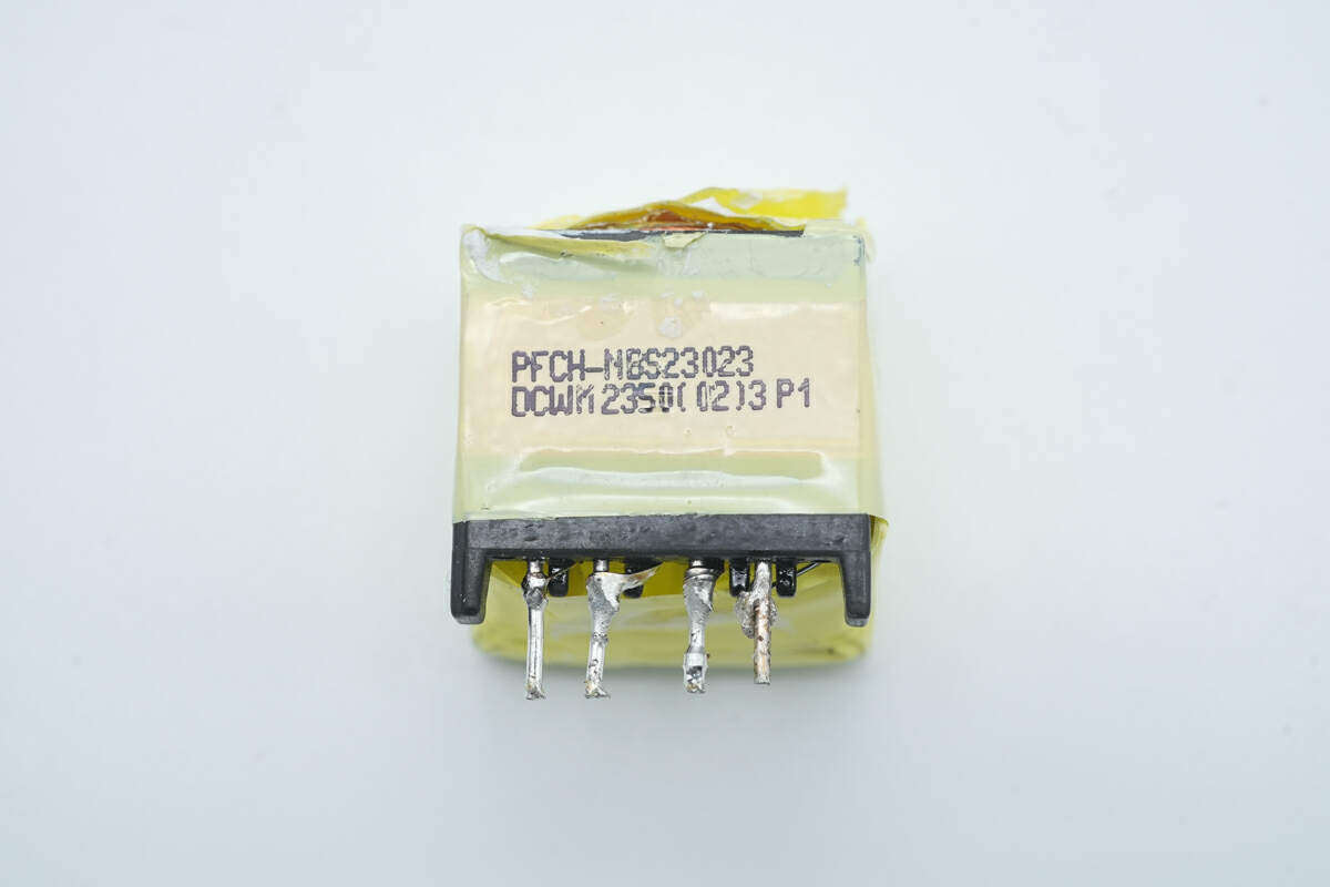
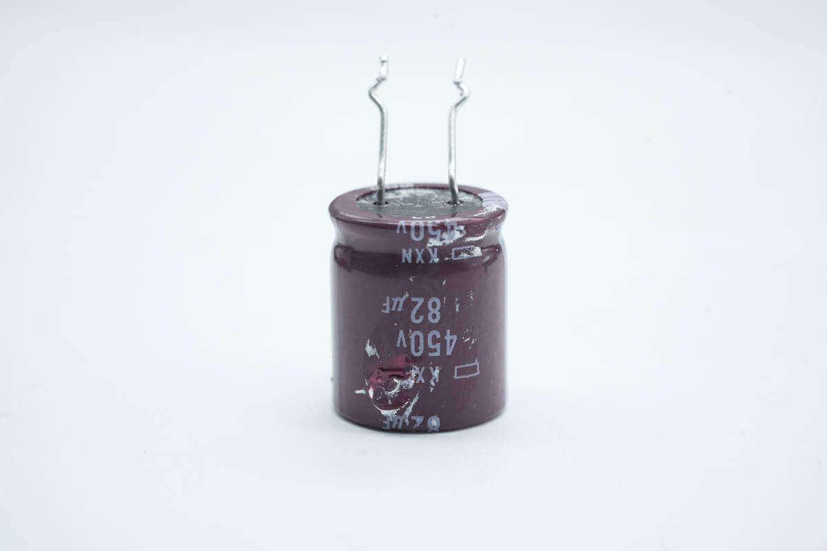
The side of PCBA module is welded with high-voltage filter capacitor and transformer.
High voltage filter capacitor is from Guimigong, and the specification is 450V82 μ F.
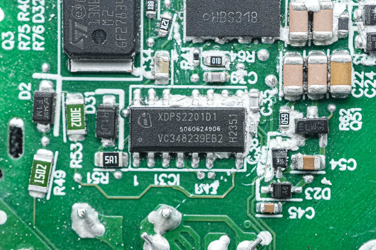
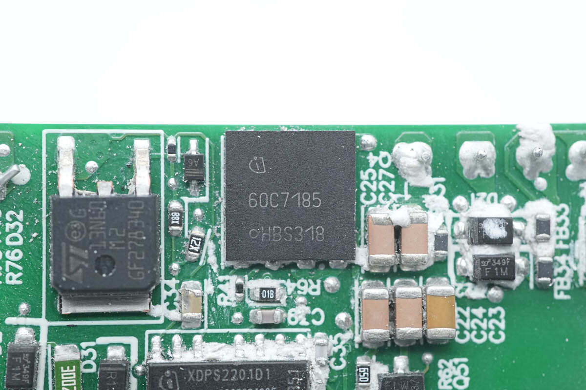
The HFB controller, XPDS2201, is a digital hybrid flyback controller from Infineon, which is internally integrated with 600V high-voltage starting circuit and high and low side MOS drive.Peak current mode control is adopted for fast load response.Based on the output current level, it can automatically switch to burst mode operation, support primary side overvoltage protection, standby power consumption<75mW, configure parameters through the single pin UART interface, adopt PG-DSO-14 packaging, and simplify peripheral components.
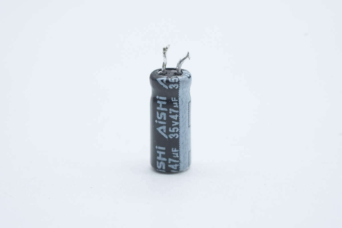
The filter capacitor supplied by the main control chip is from Aihua, and the specification is 35V47 μ F.
The switch tube is from Infineon, model IPL60R185C7, NMOS, withstand voltage 650V, conductivity 185m Ω, and is packaged with ThinPAK8 * 8.
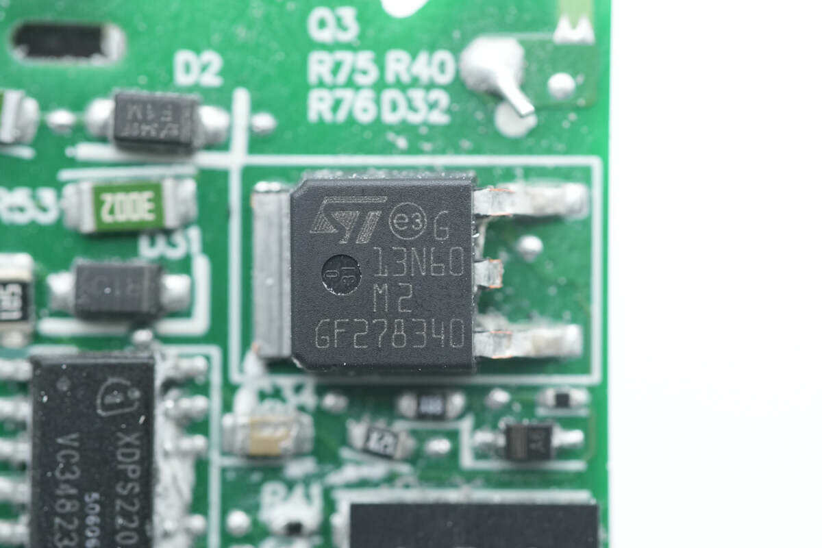
The HFB upper tube is from ST STD13N60M2, NMOS, 650V withstand voltage, 380m Ω conductivity, and DPAK packaging.
Side welding switch transformer and output filter capacitor.
The magnetic core of switching transformer shall be tightly wrapped with adhesive tape for insulation.
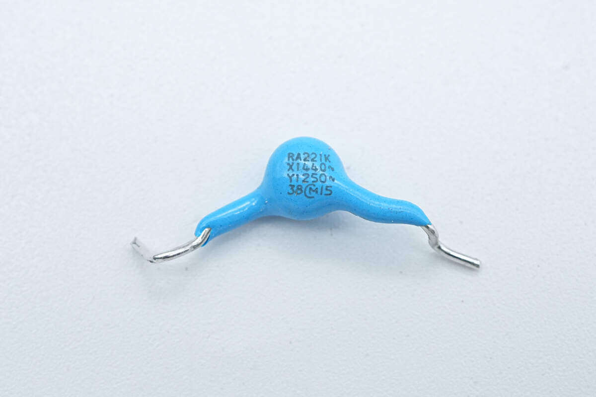
Close up of blue Y capacitor.
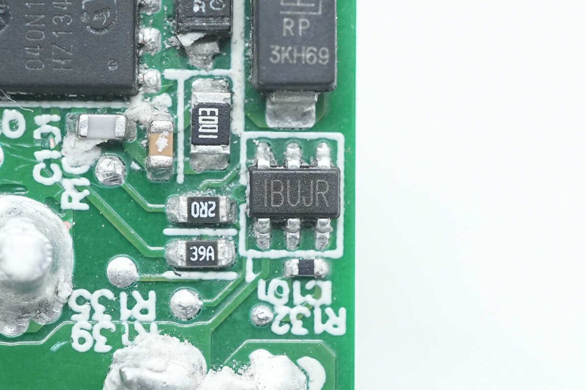
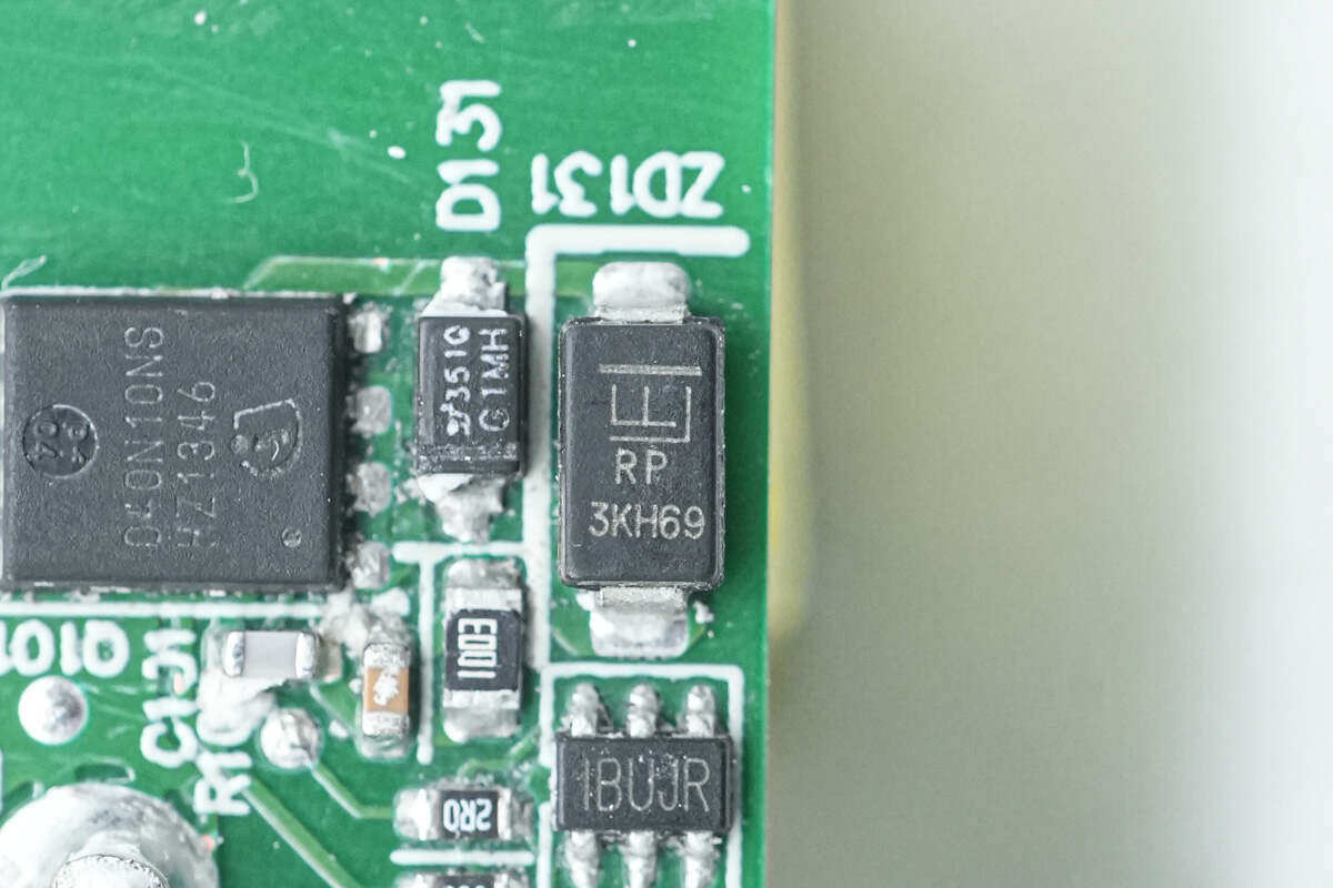
Guangbao LTV1004 optocoupler is used for output voltage feedback regulation.
The synchronous rectifier controller is from MPS core source semiconductor, silk screen IBUJR, and the actual model is MP6951. It supports DCM, CCM, QR, ZVS working modes, and also supports ACF active clamping flyback and HFB hybrid flyback. The operating frequency can reach 1MHz. It supports driving GaN synchronous rectifier tubes, supports high side and low side applications, and is packaged with TSOT23-6.
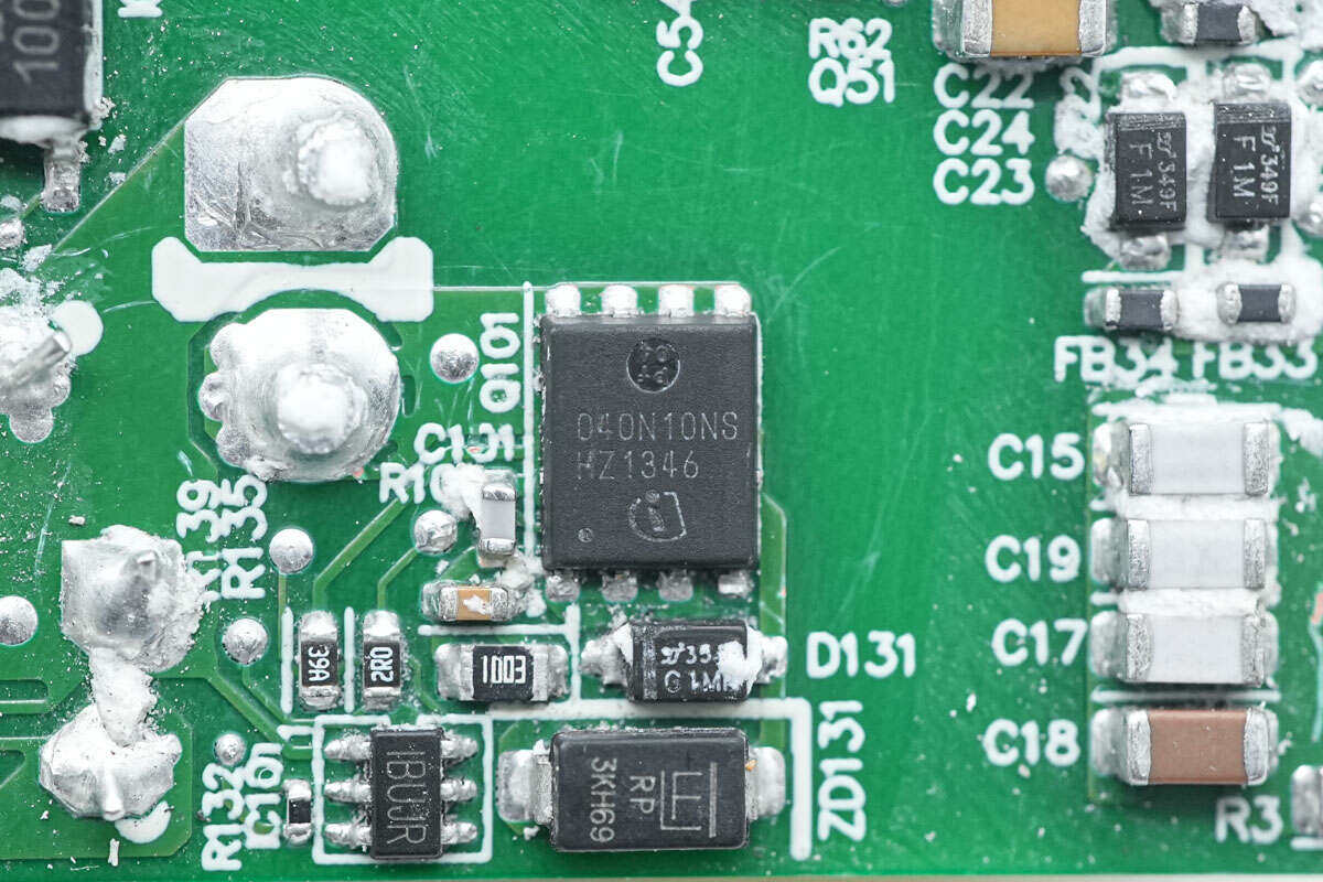
The synchronous rectifier tube is from Infineon, model BSC040N10NS5, NMOS, withstand voltage 100V, conductivity 4m Ω, and is packaged with PG-TDSON-8.
One TVS diode from Lite, model SMAJ70A, is used to absorb surge overvoltage.
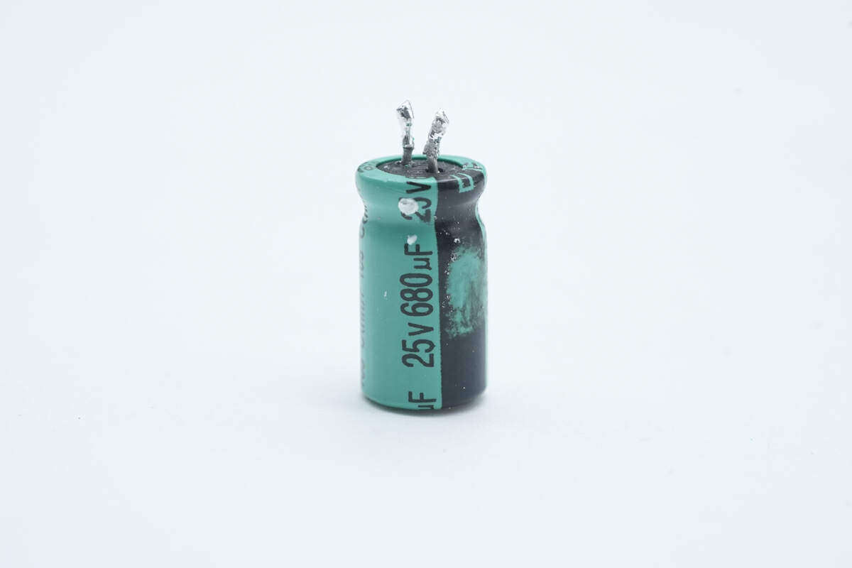
The specification of output filter solid capacitance is 680 μ F25V.
Filter electrolytic capacitors have the same specifications.
The protocol IC adopts Weiquan WT6636F, which is a protocol chip certified by USB-IF Association USB PD3.0 (PPS), and has passed Qualcomm QC4+certification.The WT6636F supports USB PD3.0 and PPS, line loss compensation and multiple protection functions.The internal integrated 10bit ADC is used for voltage and current detection, with a built-in 8051 core microcontroller and a built-in discharge MOS tube.
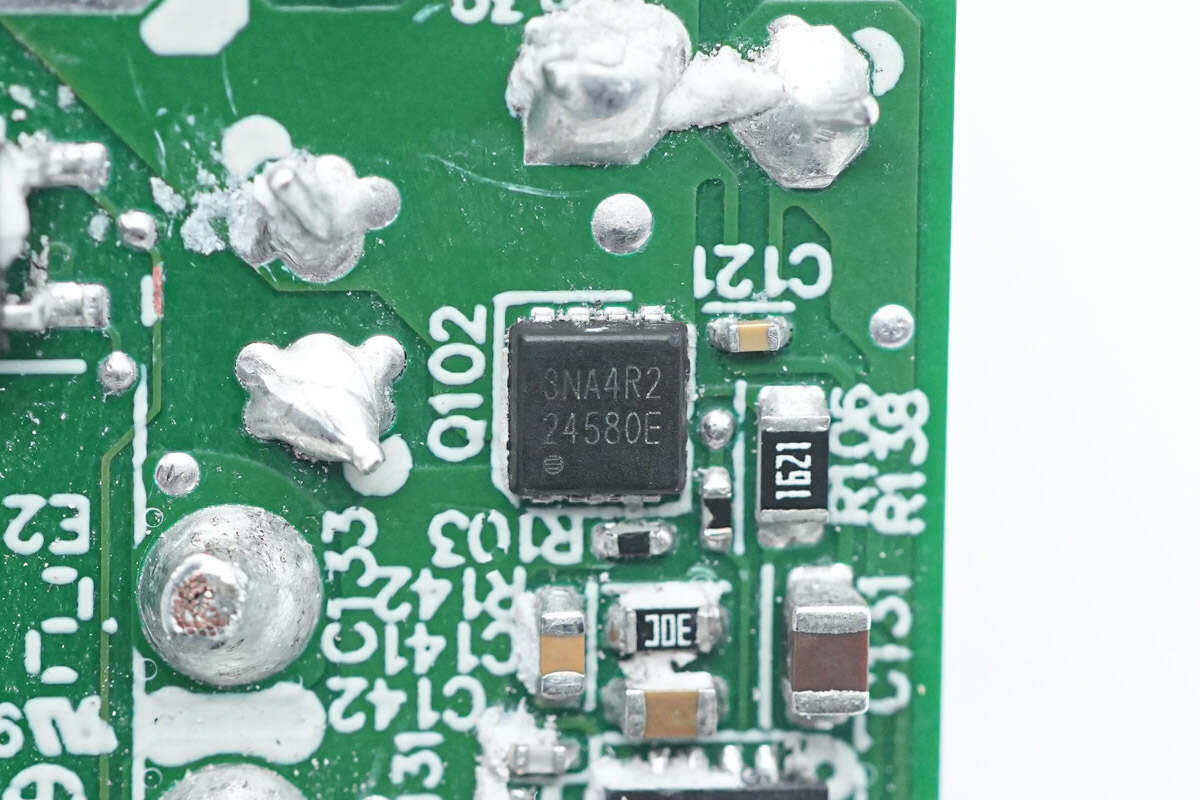
VBUS switch tube is from Fuding Advanced, model AP3NA4R2YT, NMOS, withstand voltage 30V, conductivity 4.2m Ω, and PMPAK3 * 3 packaging.
Take a look at all of them and have a family photo.
Disassembly summary of charging head network
Lenovo's 100W GaN power adapter uses the national standard three pin pin. On the one hand, it has the grounding function to prevent the metal shell laptop from numbing hands. It is also more stable to use on the wall and is not easy to drop.The adapter comes with a 1.8m long output line, which can meet most applications.The measured adapter supports 100W PD fast charging and 21V3A PPS fast charging.
The charging head network learned through disassembly that Lenovo's power adapter uses the PFC+HFB architecture, the PFC controller uses the Ansome NCP1623, and the Gallium Future G1N65R150PB-H GaN switch tube is used.The HFB circuit is composed of Infineon XDPS2201 controller and two MOS transistors.
Gallium depletion GaN switches in the future support the use of traditional silicon MOS controllers, with good versatility and compatibility.The transformer and power device are filled with glue to enhance heat conduction.The adapter PCBA module is wrapped with aluminum sheet to enhance heat dissipation, optimize the heat dissipation performance for notebook charging and high-power continuous output scenarios, and reduce the use temperature rise.