RomanceIntroduced a two in one fully rechargeable mobile power supply with a power bank and charger, which is built into the mobile power supply10000mAhBattery, with1A1COutput interface, USB-C interface supports in charger mode67WFast charging, USB-A interface supports 22.5W fast charging.When two ports are used at the same time, it supports 45W+18W power automatic distribution, and can charge mobile phones and laptops at the same time.
In the mobile power mode, the USB-C interface supports 30W fast charge, the USB-A interface supports 22.5W fast charge, and the USB-C interface also supports 18W fast charge input to charge the mobile power.The mobile power supply is equipped with a folding power pin for easy storage and carrying. The side of the body is equipped with a hidden LED power indicator light and touch buttons for better use experience.It is brought by the charging head network belowRomanceTake a look at the design and materials of this two in one mobile power supply.
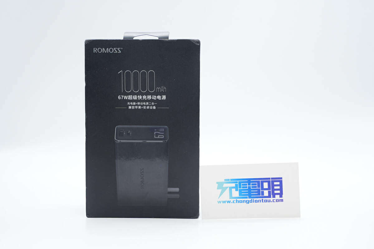
Romance67WUnpacking of super fast charging mobile power supply
The front of the box is printed with the ROMOS brand, product name, selling points and appearance.
The back is printed with a brief introduction to the mobile power supply, specifications and business information.
A close-up of the parameters of the mobile power supply, which will be introduced in the product demonstration link below.
Mobile power supply, data cable and user manual are included in the package.
The attached data line is USB-C to USB-C line. The head shell and net tail are of integrated design. The front and back are respectively designed with the ROMOS brand and transmission logo.
The measured data line is about 102.5cm long.
Romance67WThe super fast charging mobile power supply adopts PC fireproof plastic shell, and the main body shell is sprayed with metallic gray paint, which is full of texture. The edge of the output end panel is decorated with bright surface, improving the product's delicacy.
The front center of the fuselage is printed with the ROMOS brand.
The mobile power parameter information and relevant marks are printed on the side. The mobile power has passed CCC certification and can be carried on the aircraft.
One end on the same side is equipped with foldable national standard pins.
The other side is equipped with touch power key and indicator light.
In the charger mode, the indicator lights up green after power on to give the user a prompt.
Under the mobile power module, it acts as the power indicator, and the light color also turns red, which is convenient for users to distinguish.
The edge of the output end of the fuselage is treated with a high gloss surface, and the shell is printed with67WGaN lettering.
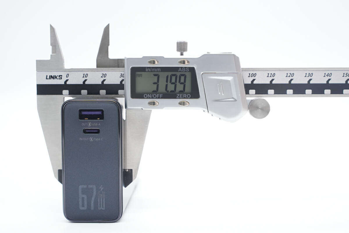
Configuration at this end1A1CDual USB interface, the interface rubber core is purple.
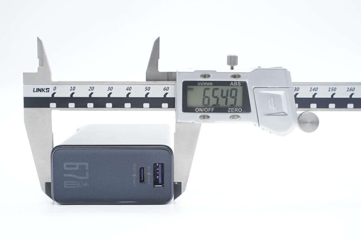
The measured length of the mobile power supply body is 125.31mm.
The width is 65.49mm.
The thickness is 31.99mm.
The size of the product in the hand is intuitive.
In addition, the weight of the mobile power supply is about 372g.
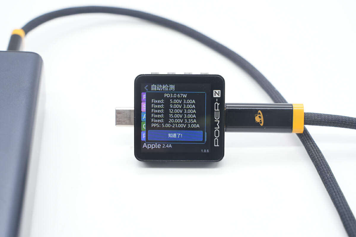
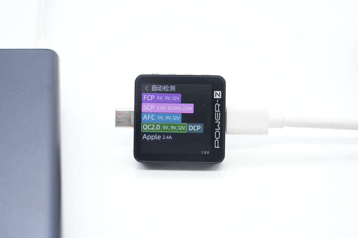
In the charger mode, the Type-C interface measured by ChargeLAB POWER-Z KM003C supports the charging protocols of FCP, SCP, AFC, QC2.0/5, PD3.0, PPS, DCP and Apple 2.4A.
PDO message shows that Type-C interface also has five sets of fixed voltage gears: 5V3A, 9V3A, 12V3A, 15V3A, 20V3.35A, and 5-21V3A, one set of PPS voltage gears.
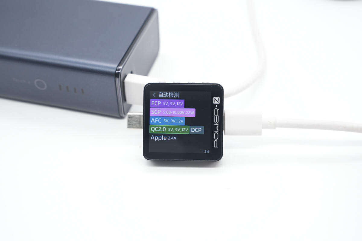
It is measured that the USB-A interface supports the charging protocols of FCP, SCP, AFC, QC2.0, DCP and Apple 2.4A.
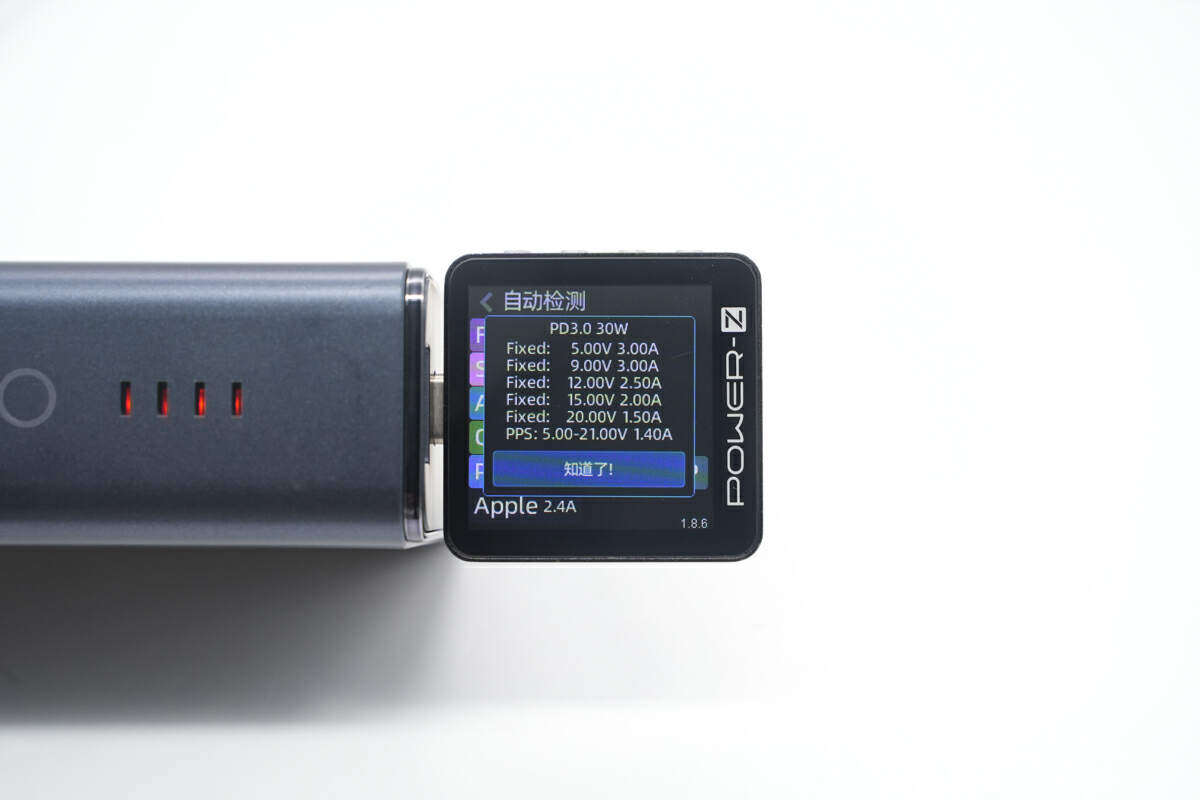
In the mobile power mode, it is measured that the Type-C interface supports the charging protocols of FCP, SCP, AFC, QC2.0/4+, PD3.0, PPS, DCP and Apple 2.4A.
PDO message shows that Type-C interface also has five groups of fixed voltage gears: 5V3A, 9V3A, 12V2.5A, 15V2A, 20V1.5A, and 5-21V1.4A, one group of PPS voltage gears.
Finally, it is measured that the USB-A interface supports the charging protocols of FCP, SCP, AFC, QC2.0, DCP and Apple 2.4A.
ROMES 67W Super Fast Charging Mobile Power Unpacking
After seeing the unpacking and display of the Romance super fast charging mobile power supply, let's take a look at the internal design and materials.
First pry off the side cover plate of the mobile power supply, and fix the cover plate by pasting.
The inner cover plate is fixed by screws.
Unscrew the fixing screws to separate the movement and the plastic housing.
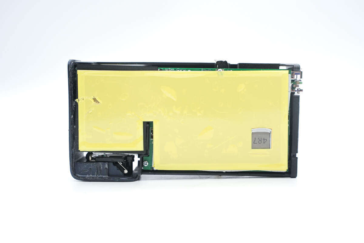
The internal PCBA module and battery pack are fixed with plastic frames.
The other side is provided with a folding pin.
The frame is hollowed out to hold the battery and reduce the thickness.
A heat conduction pad is arranged on the back, and the corresponding inductance position is hollowed out to reduce the thickness.
Touch the button to paste conductive cloth to contact the shell.
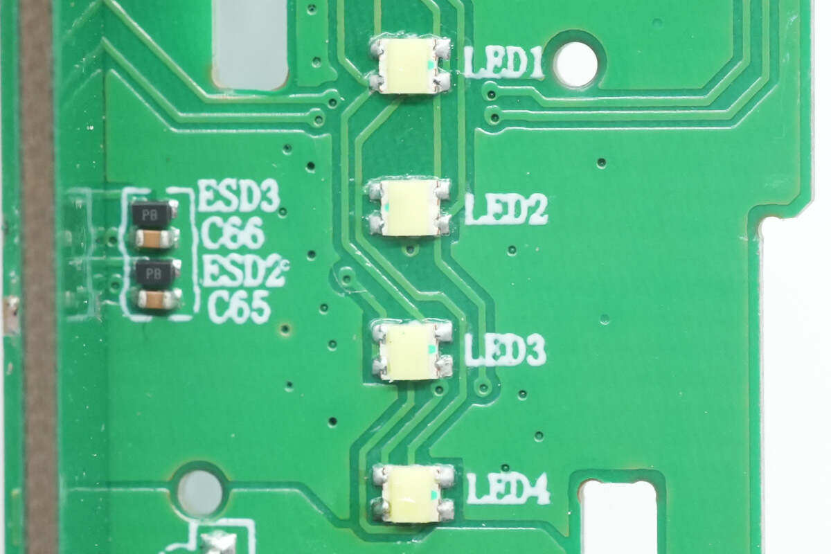
Close up of four LED power indicators.
The PCBA module is fixed on the frame by screws.
Unscrew the fixing screws and take out the internal PCBA module.
The fold pin is connected to the PCBA module for power supply through a wire.
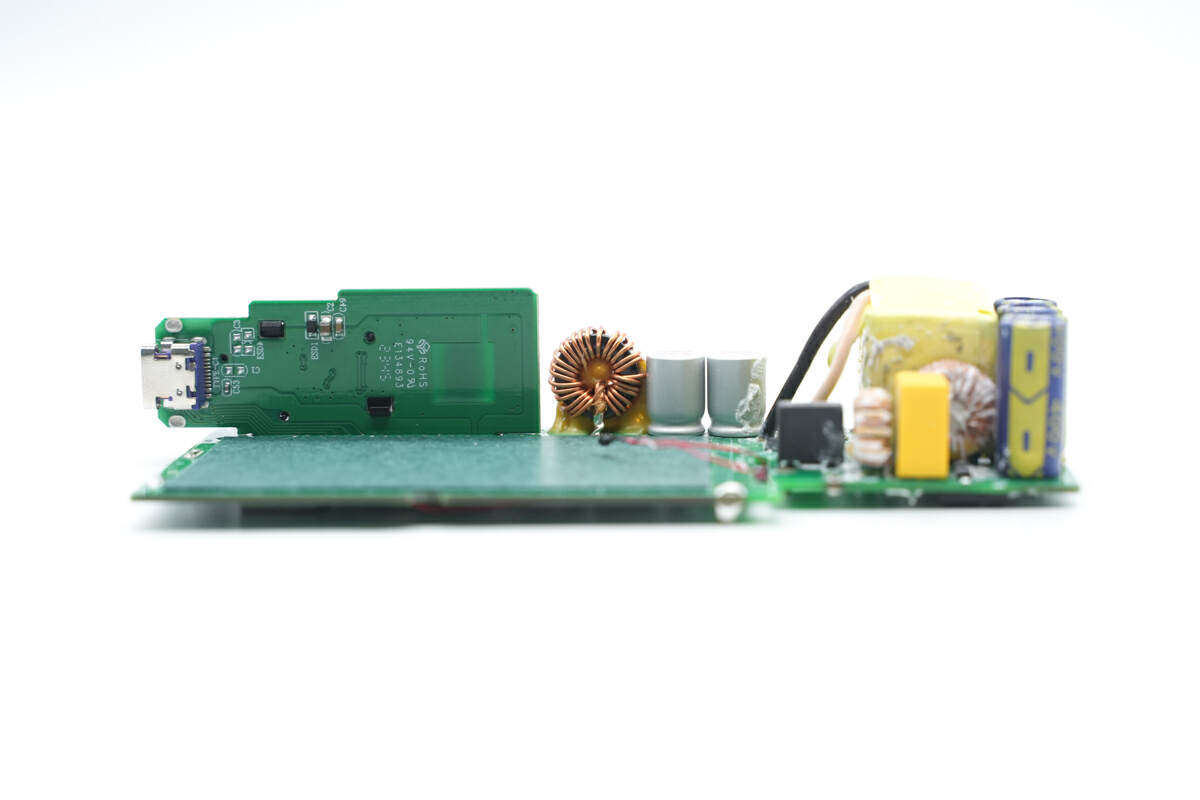
The front of the PCBA module is at a glance. On the left side is the switching power supply part, four high-voltage filter capacitors are welded, and on the right side are transformers and other components, which are glued and reinforced.Two 21700 batteries are set on the right side, and the filter capacitor, magnetic ring inductance, power indicator and touch button board are set below.
At the back of the PCBA module, the left side is welded with the rectifier bridge, the GaN sealing chip, and the right side is welded with two synchronous voltage rise and fall circuits, protocol chips, and multiple MOS tubes.
Through the observation of the PCBA module, it is found that the internal flyback switching power supply is used in the Luolishi 67W super fast charging mobile power supply, with a wide range of voltage output. The output voltage is fed back by the protocol chip through the optocoupler, and output by the USB-C interface.And output to the USB-A port through the synchronous voltage rise and fall circuit, or charge the battery.
When the mobile power supply is in the state, the battery is output through the synchronous voltage rise and fall circuit. There are two synchronous voltage rise and fall circuits in total. The internal switching power supply and synchronous voltage rise and fall chip are from Nanxin Technology.Now let's start from the input to understand the information of each device.
Remove two 2100 batteries by welding. A thermistor is installed on the PCBA module to detect the temperature of the battery, and highland barley paper is pasted between the battery and PCB for insulation.
The two batteries are connected in series and fixed by glue.
The positive and negative electrodes of the battery are connected by spot welding with nickel sheets.
Paste foam cushion insulation on the other end.
The battery is a 21700 battery with a model of N21700CG-50D and a rated voltage of 3.6V, capacity of 5Ah and energy of 18Wh.
Clean the glue of the PCBA module, and let's learn about the materials and design of this power supply.
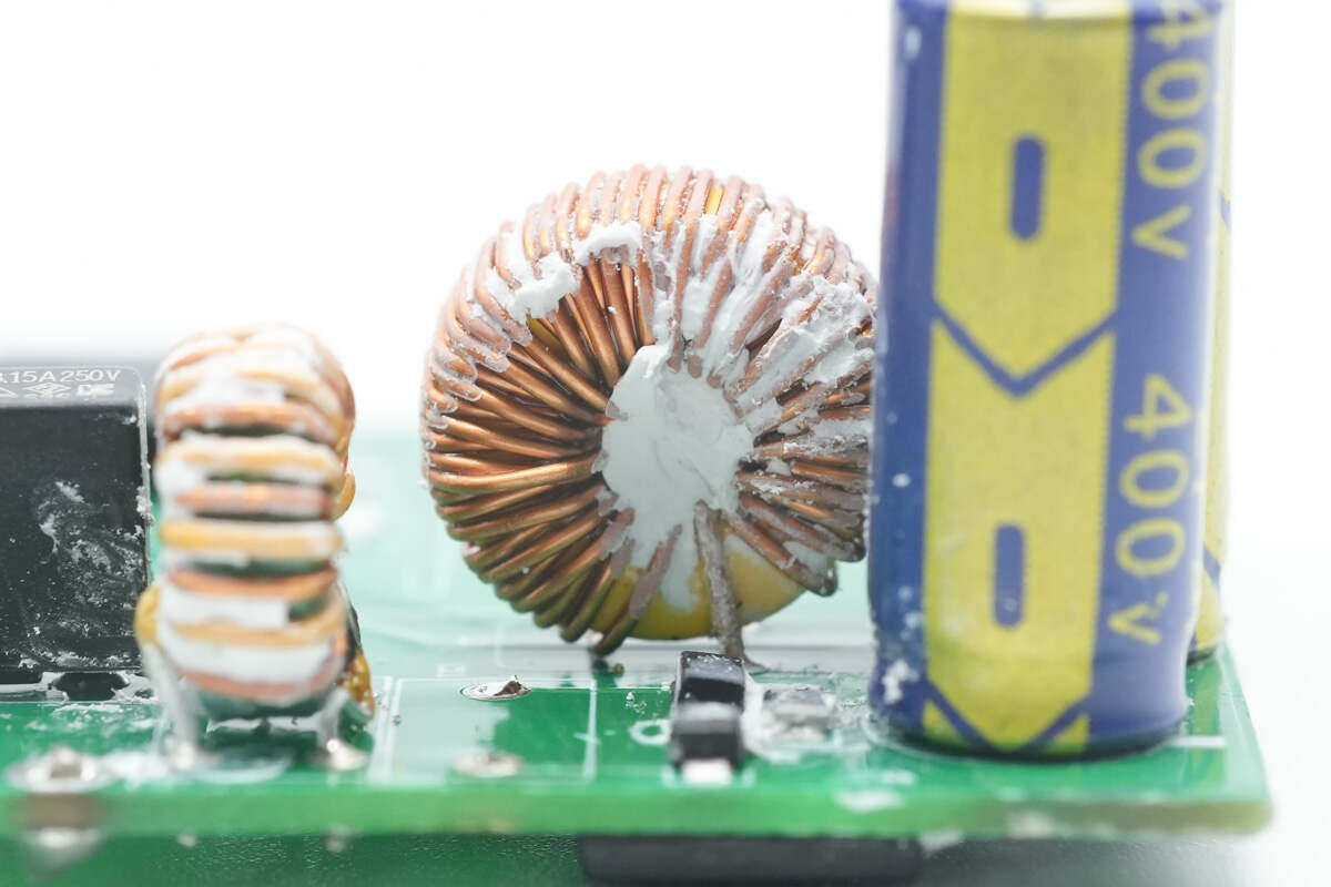
The side view of PCBA module is as follows: the right side is equipped with fuse, common mode inductance, safety X2 capacitor and high-voltage filter capacitor.
The input fuse specification is 3.15A250V.
Common mode inductance is wound with enameled wire and insulated wire.
The safety gauge X2 capacitor is from Chengdong, and the specification is 0.22 μ F.
The model of rectifier bridge is ULBF810, and the specification is 8A 1000V.
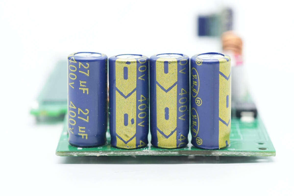
Four high-voltage filter capacitors are welded on the side of the PCBA module. The capacitors are from Yuguang Electronics, and the specification is 400V27 μ F. The four capacitors have a total capacity of 108 μ F.
The differential mode inductor adopts magnetic loop winding.
The primary master chip is from Nanxin Technology, which uses SC3057 sealed GaN chip. This chip integrates high-performance multi-mode flyback controller, GaN driver, GaN switch, power supply and protection circuits into a heat dissipation enhanced QFN6 * 8 package.The number of external components is simplified by sealing, and the influence of parasitic parameters of traditional drive wiring on high-frequency switches is eliminated.
The SC3057 of Nanxin Technology adopts the design of separating power wiring and control wiring to reduce the impact of high-frequency switches on the control circuit. Through the optimized pad design, the charger wiring design and electrical performance are optimized to simplify the design and development.The SC3057 has a built-in 165m Ω GaN switch tube, supports 175KHz switching frequency, and supports X capacitor discharge.
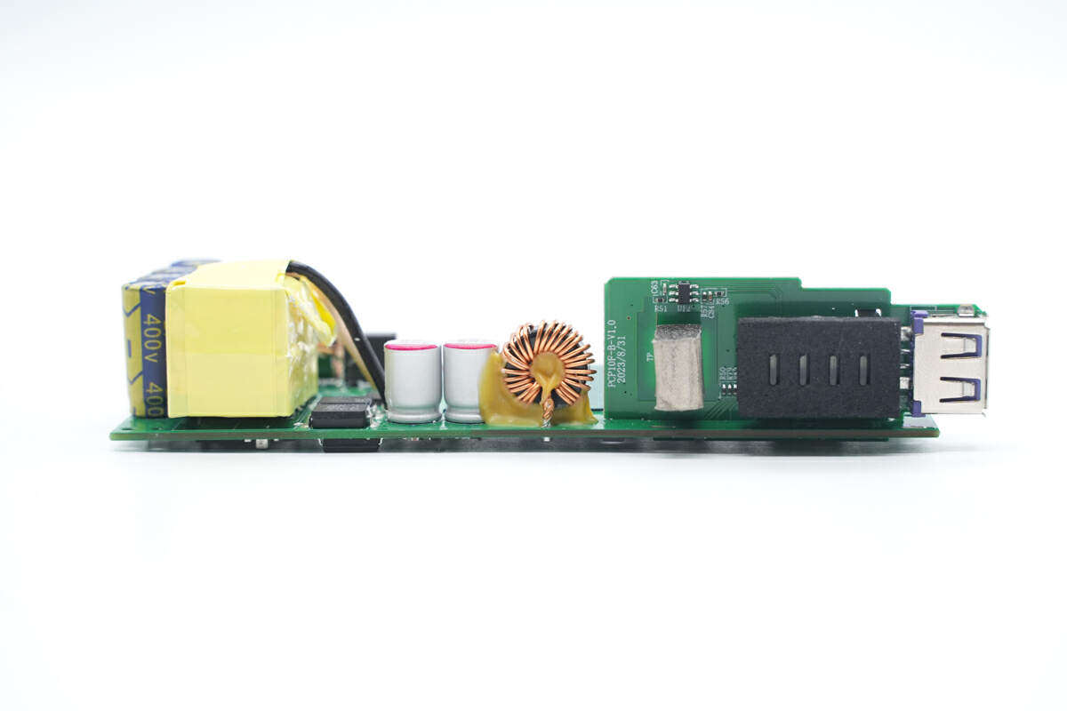
Weld transformer, SMD Y capacitor, filter solid capacitor, magnetic ring inductance and output board on the side of PCBA module.
The transformer shall be sealed with adhesive tape for insulation.
The SMD Y capacitor comes from Sichuan Teruixiang Technology Co., Ltd., which has the characteristics of small size and light weight, and is very suitable for use in high-density power products such as GaN fast charging.The part number is TMY1471M.
Teruixiang focuses on the R&D, production and sales of passive components, with a registered capital of 100 million yuan.It has two independent capacitor brands: SMD TRX and DIP TY capacitors. TRX will devote itself to the research of ceramic materials to expand the application of more categories and provide customers with more solutions.
Yiguang EL1019 optocoupler is used for output voltage feedback regulation.
The synchronous rectifier controller comes from Nanxin Technology, model SC3503. It is an adaptive on detection and fast off synchronous rectifier controller. It does not need auxiliary coil power supply, and the output voltage can be as low as 0V. The patented adaptive on detection circuit avoids the wrong opening of synchronous rectifier tubes, is compatible with multiple MOS, has ultra-low static current, and supports multiple working modes,Support high side and low side synchronous rectification, and the peripheral components are very simple.
The synchronous rectifier tube is from Ansender, model ASDM120R65N, NMOS, withstand voltage 120V, conductivity 5.3m Ω, and sealed with DFN5 * 6-8L.
The specification of two filter capacitors is 680 μ F25V.
The protection chip for the two strings of battery packs inside the mobile power supply is from Chuangxin Micro, with the model of CM1020-DC. It is a protection chip for two strings of lithium batteries. The chip has built-in high-precision voltage detection circuit and current detection circuit for battery overcharge, over discharge, discharge overcurrent, short circuit, and charging overcurrent protection.
CM1020-DC overcharge protection voltage is 4.280V, detection accuracy is 25mV, over discharge protection voltage is 2.35V, detection accuracy is 80mV.The charge discharge overcurrent protection and short circuit protection voltages are detected on the MOS tube resistance used.The chip is packaged with SOT23-6.
Chuangxin Micro CM1020-DC data information.
The battery equalization chip is also from Chuangxin Micro, model CM1010-A. The chip is internally integrated with high-precision voltage detection circuit and delay circuit. By detecting the battery voltage, it controls the conduction of external MOS tubes, and accesses the resistance for equalization to meet the application of multi string lithium ion battery packs.
The balanced open detection voltage of Chuangxin Micro CM1010-A is 4.2V, the precision is 25mV, the balanced off hysteresis voltage is 0.01V, the precision is 50mV, and the chip is packaged with SOT23-6.
Data information of Chuangxin Micro CM1010-A.
Two battery protection tubes are from Ansender, model ASDM30N65E, NMOS, withstand voltage 30V, conductivity 4.5m Ω, and sealed with DFN3.3 * 3.3-8L.
The synchronous voltage rise and fall converter for battery charging is from Nanxin Technology, model SC8812A, which is a high-efficiency synchronous two-way voltage rise and fall chip. It supports voltage rise or voltage drop to charge 1 to 4 batteries, complete charging and discharge control, and support various voltage conversion and charging status indication;Built in 10bit ADC, I2C numerical control interface is adopted, output voltage and current limiting value are configured, and simplified external devices help reduce the board area.
The two MOS tubes at the input end are from Andersen Semiconductor, the model is ASDM30N55E, NMOS, the withstand voltage is 30V, the resistance is 4.8m Ω, and the DFN3.3 * 3.3-8 is used for packaging.
Close up of MLCC filter capacitor connected in parallel at the input end.
The synchronous voltage rise and fall inductance is wound with magnetic ring and fixed with glue.
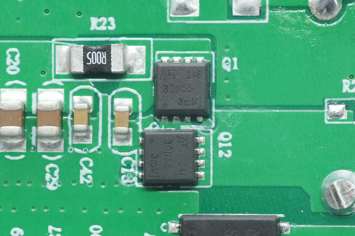
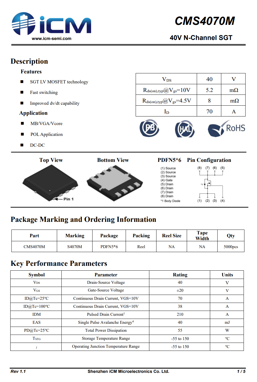
The two MOS tubes at the output end are from the core maker, with the model of CMS4070M, NMOS, withstand voltage of 40V, conductivity of 5.2m Ω, and are packaged with PDFN5 * 6.
Chuangxin Micro CMS4070M data information.
The MLCC capacitors in parallel are used for output filtering.
The switch tube used to output VBUS control is from Chuangxin Micro, model: CMT30P47K, PMOS, withstand voltage: - 30V, resistance: 7.3m Ω, packed with PDFN3.3 * 3.3, and connected in series with two pieces in opposite direction.
Chuangxin Micro CMT30P47K information.
The other two CMT30P47K MOS tubes are used for battery charging control.
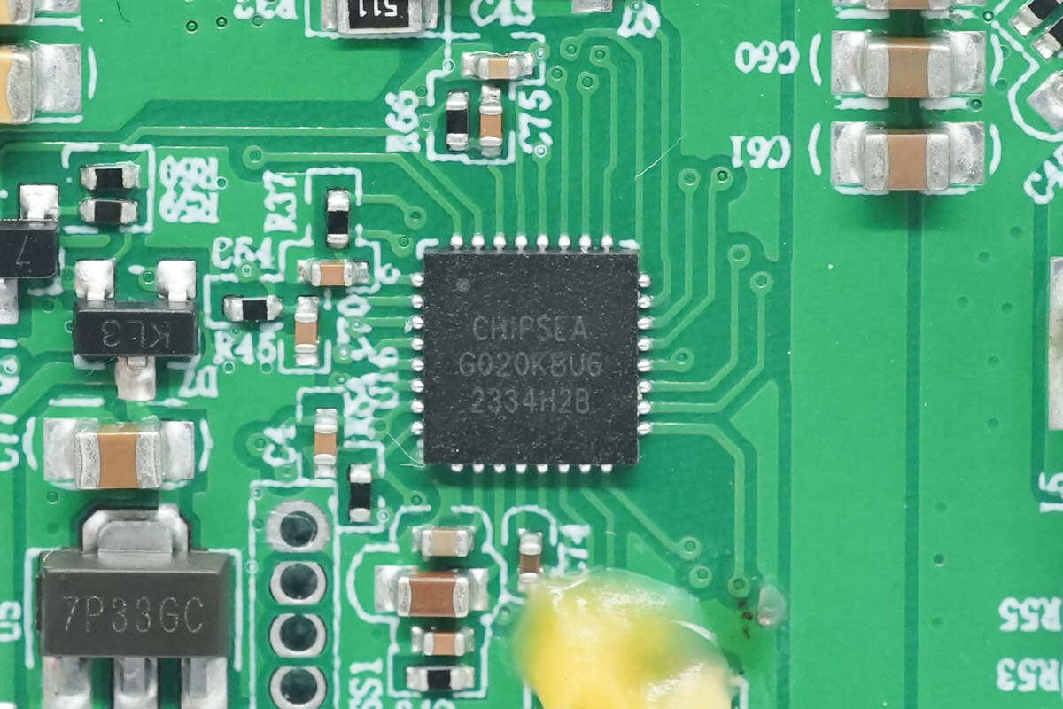
The USB PD protocol chip comes from Core Sea Technology, with a model of CS32G020K8U6. It is a USB-C controller that supports USB-C and PD3.0 launched by Core Sea Technology. The chip is suitable for PC power adapter, mobile phone fast charge charger, high-power mobile power supply, car charger, USB HUB and other fields.
Core Sea CS32G020 has built-in ARM M0 core, 48MHz main frequency, built-in 64K program memory, 4KB LDROM, 8K SRAM, supports a wide range of industrial control applications and high-performance processing scenarios, and provides QFN24 and QFN32 packaging.
The voltage stabilizing chip screen printed 7P33GC is used to power the protocol chip.
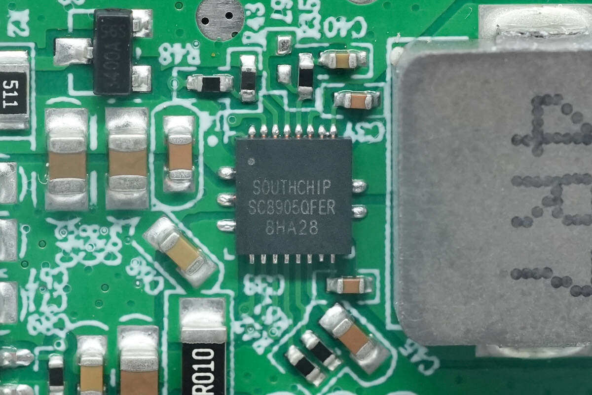
The internal voltage rise and fall converter of the mobile power supply is from Nanxin Technology, model SC8905, integrated switch tube inside the chip, supporting 2.7-22V input voltage, supporting 2-4 lithium battery charging management, and supporting reverse discharge output.SC8905 has I2C interface, which supports setting charging and discharging mode, charging current, reverse discharge voltage, current limit and switching frequency through I2C interface. The chip has built-in overcurrent protection, overvoltage protection, undervoltage protection, output short circuit and overheat protection functions.
Nanxin Technology SC8905 information.
4.7 μ H alloy inductance close-up, 10 * 10mm large size is used to reduce loss and improve conversion efficiency.
The output VBUS switch tube is from Guanyu, model KS3518HB, dual PMOS, withstand voltage - 30V, conductivity 16m Ω, and is packaged with SOP8.
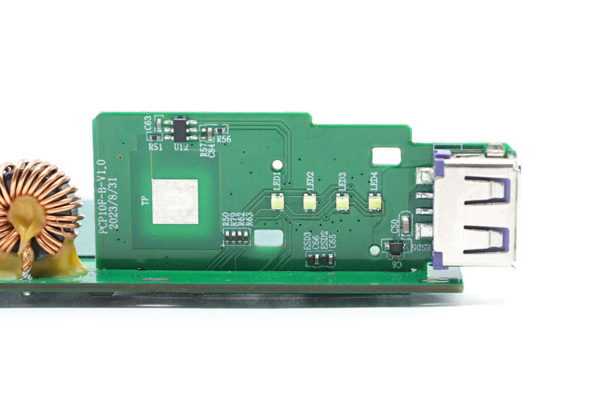
The touch detection chip, SMD LED indicator and USB-A mother seat are welded on the outside of the output small board.
The other side is welded with USB-C mother seat.
Touch detection chip silk screen 1281A.
Four power LED close-up display, supporting multiple color display.
The USB-C mother seat is fixed by via welding, and the purple tongue is clamped with steel sheet.
The USB-A female seat adopts purple tongue, and the positive and negative poles are widened to support high current fast charging.
Take a look at all of them and have a family photo.
Disassembly summary of charging head network
Romance's super fast charging mobile power supply is designed as a two in one charger+power bank. The built-in GaN charger supports 67W fast charging output, and the mobile power supply is10000mAhCapacity, support 30W fast charging output.The mobile power supply has a 1C1A output interface, supports 67W output power in the charger mode, and supports 45W+18W automatic power distribution. The power bank mode supports 30W output power to meet the daily charging of mobile phones, tablets and laptops.
According to the disassembly of the charging head network, this mobile power supply is equipped with two strings of 21700 batteries. The batteries are from BYK, with a capacity of 5000mAh, and are equipped with battery protection circuits and thermistors.Among them, the battery protection chip is from Chuangxin Micro, model CM1020-DC, and is also equipped with a battery equalization circuit, which uses Chuangxin Micro CM1010-A for battery equalization control.
The mobile power supply is composed of GaN fast charging circuit and mobile power circuit. The GaN fast charging circuit is composed of Nanxin SC3057 GaN sealing chip and SC3503 synchronous rectification controller. Nanxin SC8812A synchronous voltage rise and fall controller is used for USB-A output and battery charging, and the output voltage is controlled by the Core Sea CS32G020K8U6 protocol chip.
The mobile power circuit uses the SC8905 synchronous voltage rise and fall converter of Nanxin Technology for voltage conversion, in which the internal synchronous voltage rise and fall switch tube uses the Chuangxin Micro CMS4070M, and the MOS tube used for battery charging and USB-A interface switching uses the Chuangxin Micro CMT30P47K.The mobile power supply has compact internal design, solid materials and practical functions.