Chengxin Micro launched a65WGallium nitrideFast charging reference design, this reference design has 1C1A output interface, USB-C interface support65WFast charging output.This reference design adopts Chengxin Micro CX75GD015EGallium nitrideThe sealing chip and CX7539F synchronous rectification chip greatly simplify the circuit design of the charger and reduce the number of components.
CX75GD015E is sealed internallyGallium nitrideSwitch and high-performance quasi resonant controller, supporting65WApplication: CX7539F integrated synchronous rectifier tube and controller support multiple working modes and meet the six level energy efficiency requirements.The following charging head network brings Chengxin Micro65WGallium nitrideAnalyze the reference design of fast charging, and let's have a look at the design and materials of the scheme.
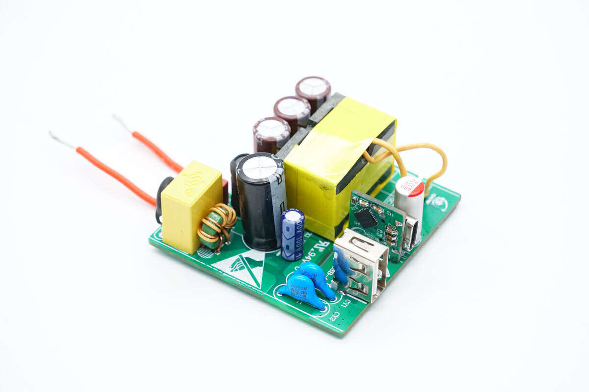
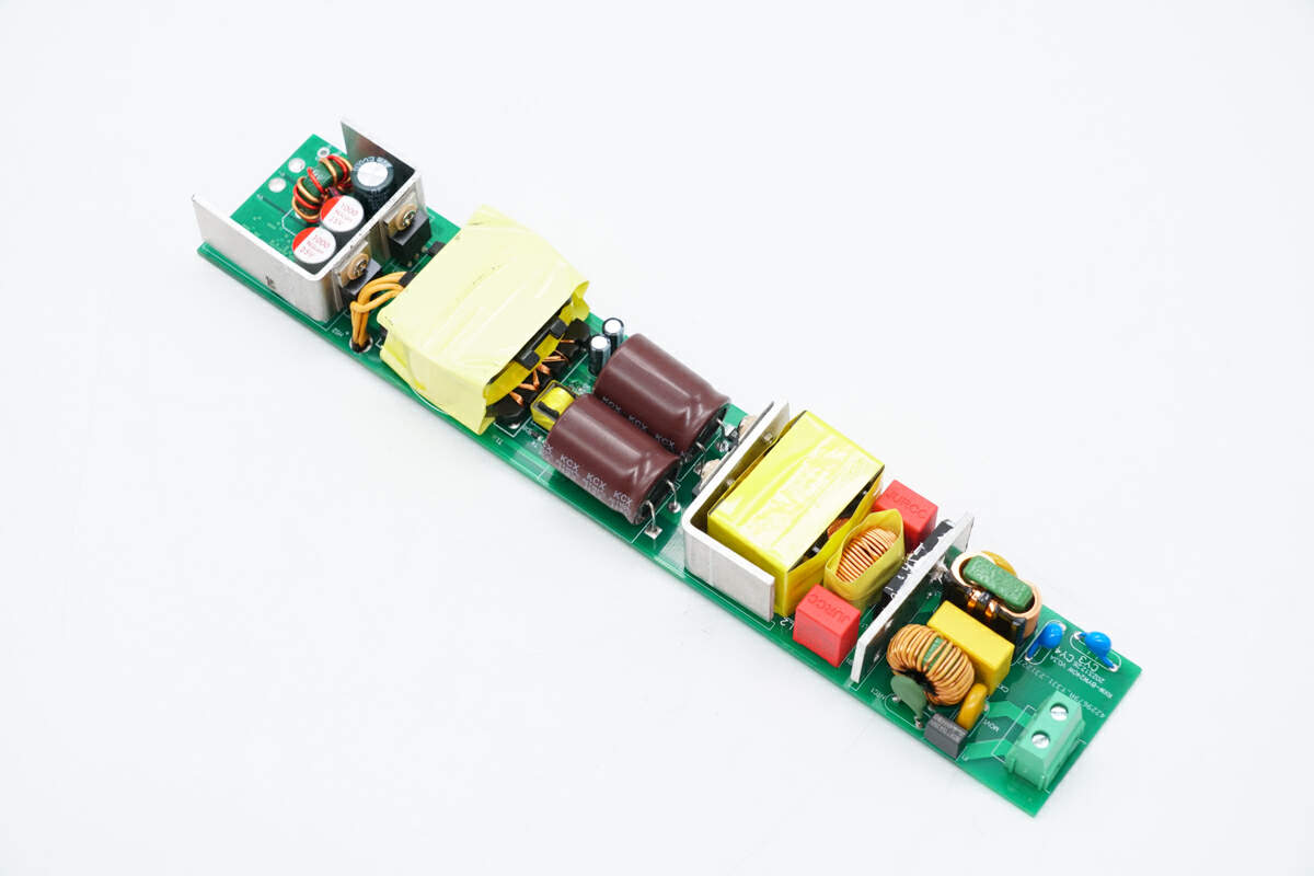
Chengxin Micro65WGallium nitrideRefer to design appearance for sealing scheme
Chengxin Micro, a 65W fast charging DEMO, arranges the components on the front of the main board in a neat and orderly manner. For the initial interstage hollowing, an insulation isolation plate can be added to improve the safety and reliability of the finished product.
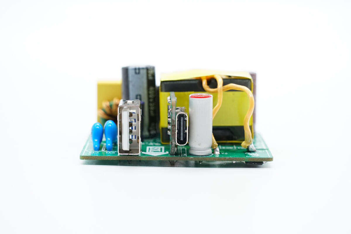
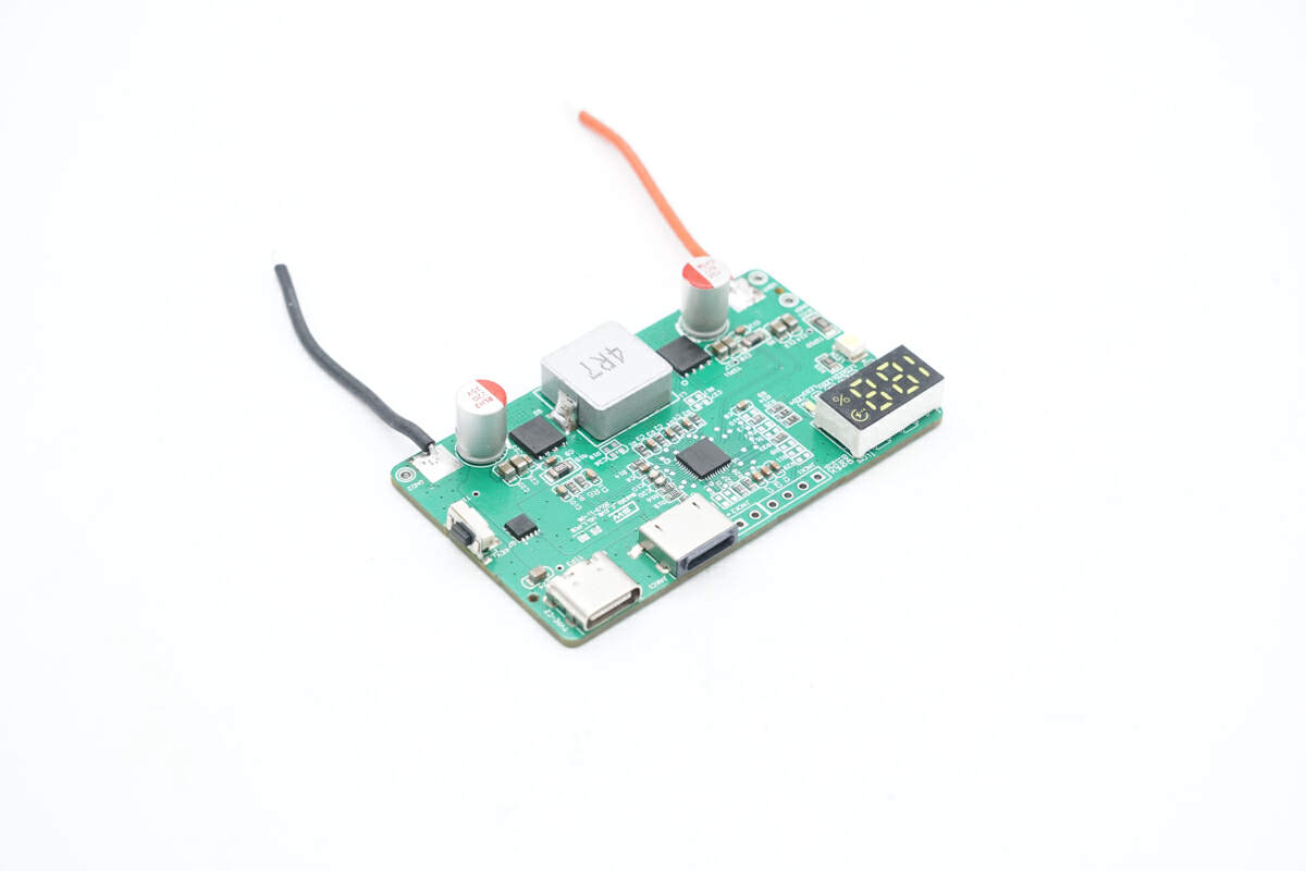
DEMO output terminal configuration1A1CDual output interface, wherein USB-C mother seat is welded with protocol small plate.In fact, the space on the motherboard is not maximized. It can be seen that the system is based on Chengxin Micro CX75GD015E+CX7539FSealed gallium nitrideThe scheme can make the power density of finished products very high, and improve the competitiveness of products in terms of small size and portability.
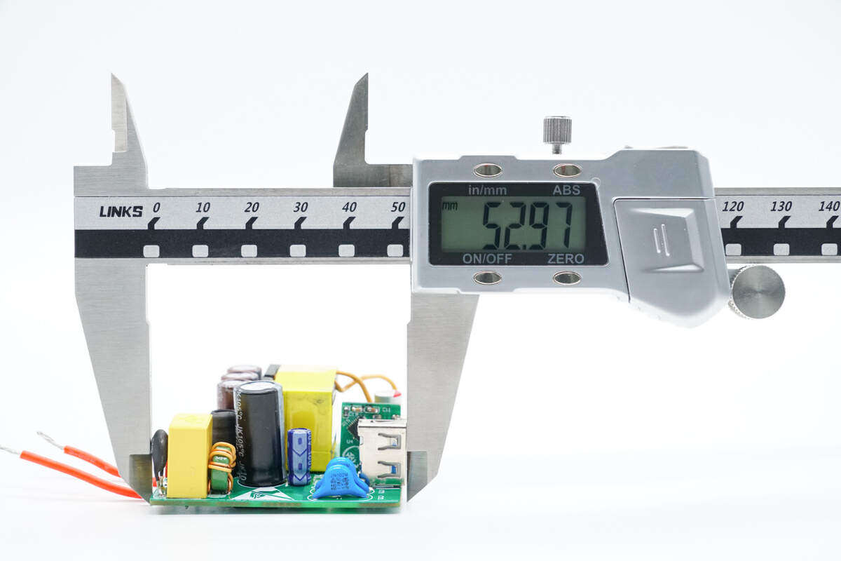
The measured DEMO length is 52.97mm.
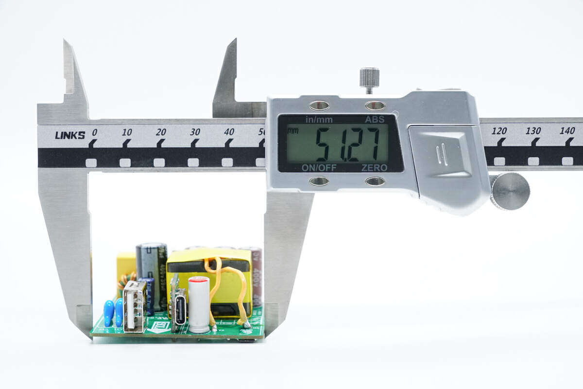
The width is 51.27mm.
The thickness is 23.85mm.
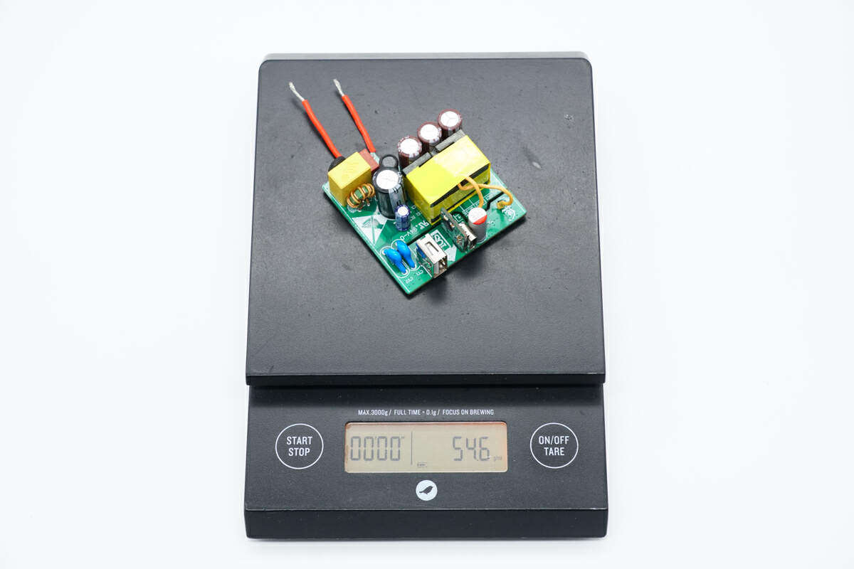
In addition, the measured net weight of DEMO is about 55g.
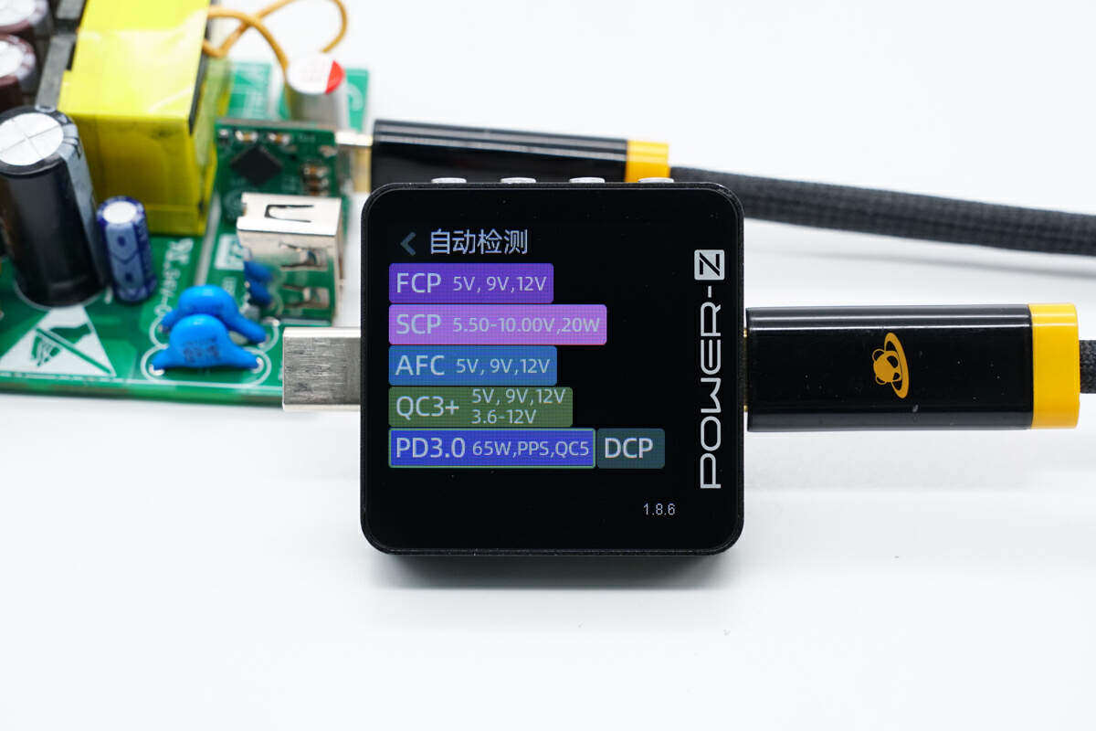
Power on the DEMO, and use the ChargerLAB POWER-Z KM003C to measure that the USB-C interface supports the charging protocols of FCP, SCP, AFC, QC3+/5, PD3.0, PPS, and DCP.
PDO message shows that the USB-C interface also has five sets of fixed voltage gears, namely 5V3A, 9V3A, 12V3A, 15V3A and 20V3.25A, and two sets of PPS voltage gears, namely 3.3-11VF3A and 3.3-16V3A.
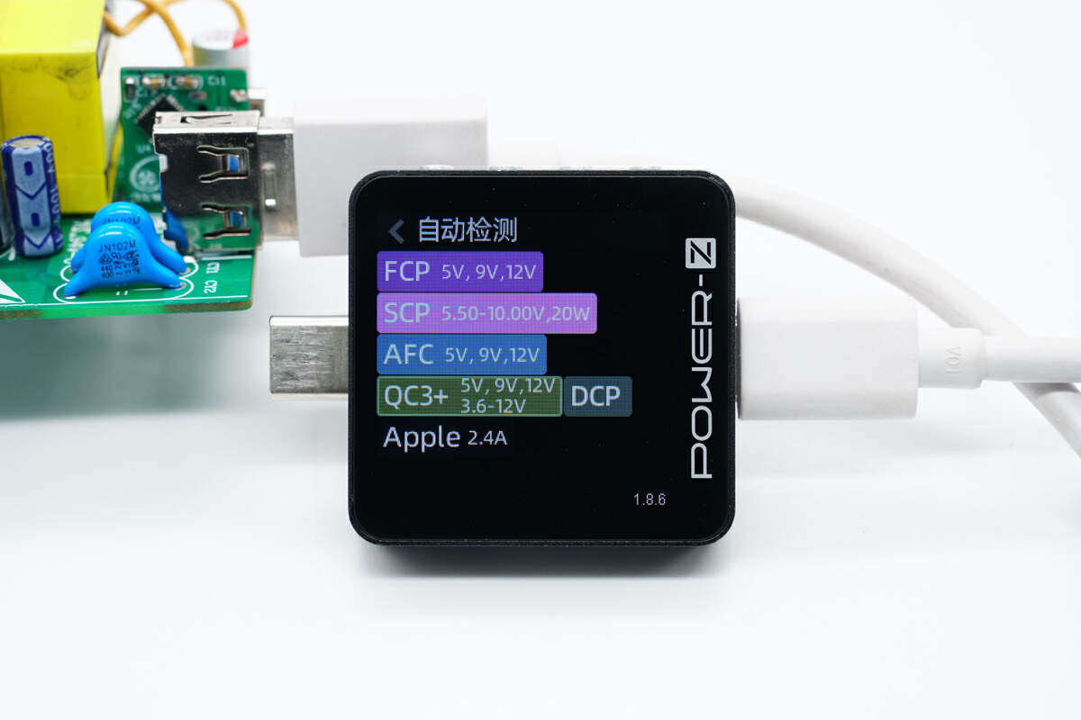
It is measured that the USB-A interface supports the charging protocols of FCP, SCP, AFC, QC3+, DCP and Apple2.4A.
Reference Design Analysis of Chengxin Micro 65W GaN Sealing Scheme
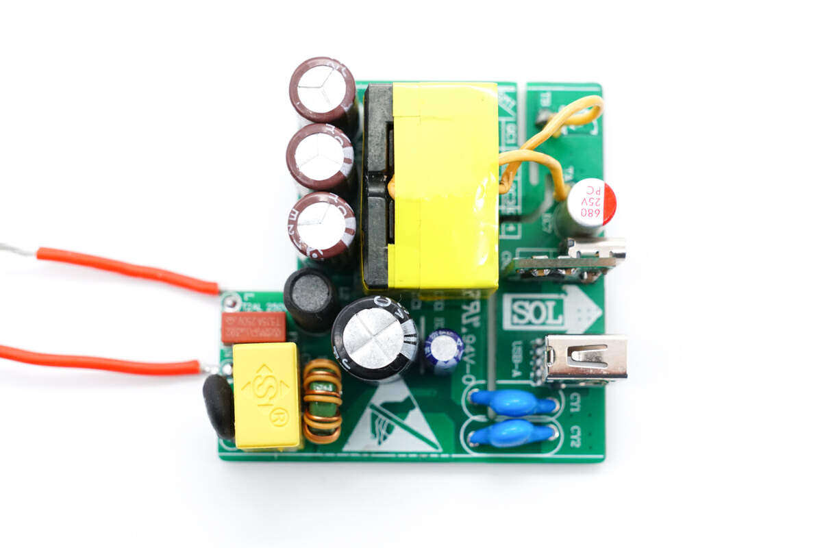
At the front of PCBA module, the lower left corner is welded with input fuse, NTC thermistor, safety gauge X2 capacitor and common mode inductance.High voltage filter capacitor is welded at the upper left corner, and transformer is welded at the right side.Weld the filter solid capacitor on the right side of the transformer, the USB-C bus plate and USB-A bus plate on the lower side, and two blue Y capacitors on the bottom.
The PCBA module is welded with a rectifier bridge on the upper back, a GaN sealing chip on the lower side, and a synchronous rectifier chip on the right side.The reference design of Chengxin Micro's gallium nitride sealing scheme is a flyback switching power supply design with a wide voltage range output. The output voltage is fed back by the protocol chip through optocoupler. Now we will analyze this reference design from the input side.
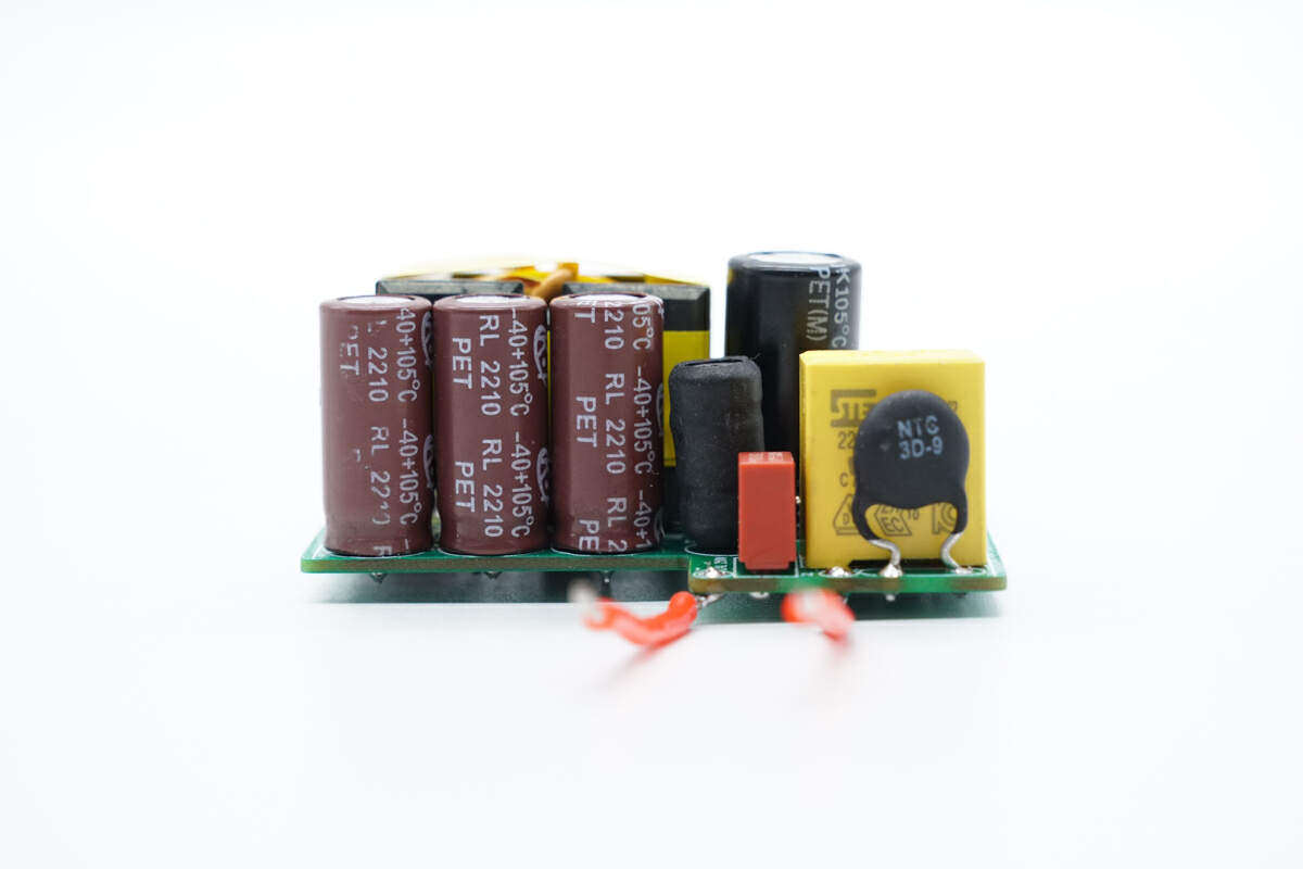
List of DEMO input terminals. The front end is equipped with delay fuse, NTC thermistor, safety gauge X capacitor, differential mode inductance, high-voltage filter electrolytic capacitor and other devices.
There are common mode inductors and power supply capacitors of the master chip on the side.
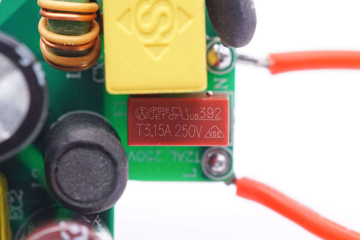
The input fuse specification is 3.15A 250V.
NTC thermistors are used to suppress the surge current of power on.
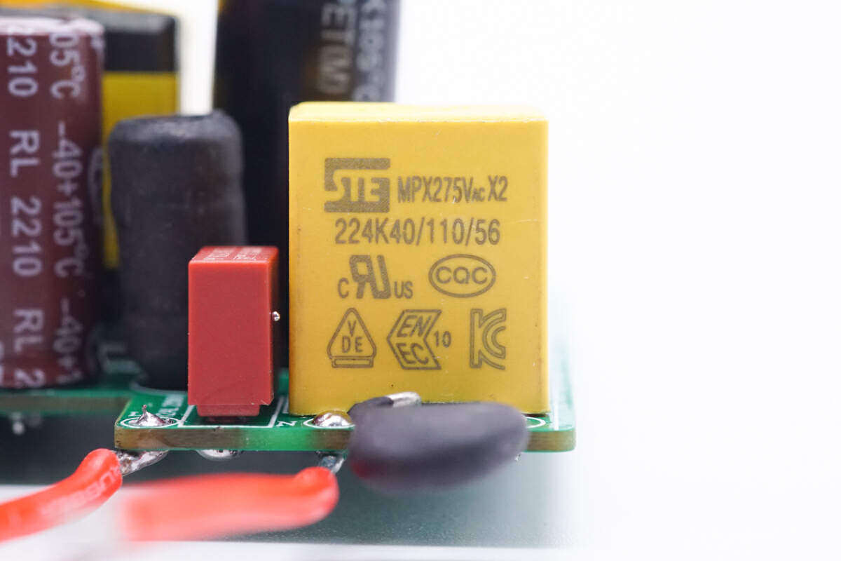
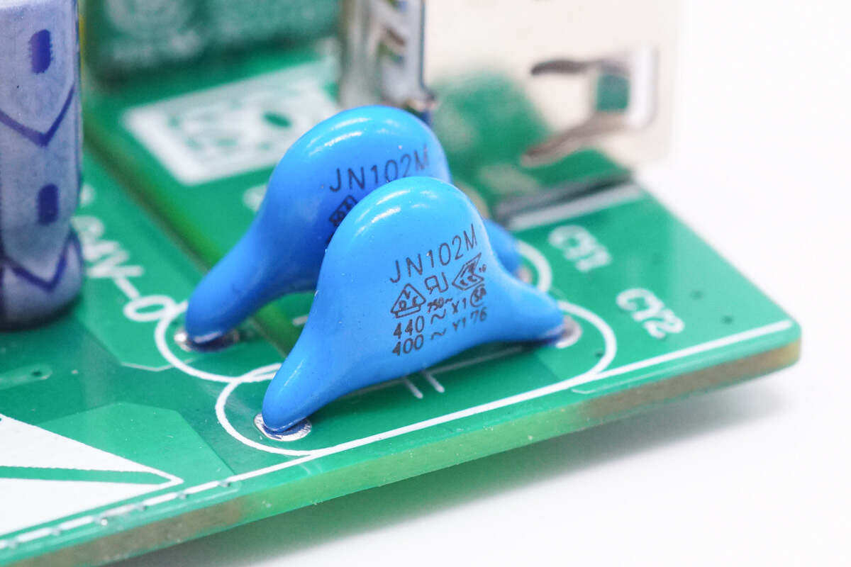
The safety gauge X2 capacitor is from STE Matata Electronics, and the specification is 0.22 μ F.
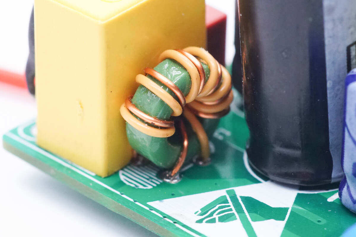
Common mode inductance is wound with enameled wire and insulated wire.
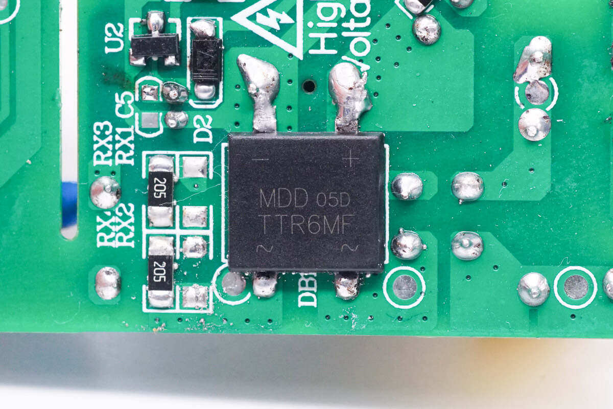
The rectifier bridge is from Chendaxing, the model is TTR6MF, which is a fast recovery rectifier bridge, and the specification is 1000V6A.
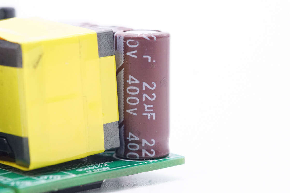
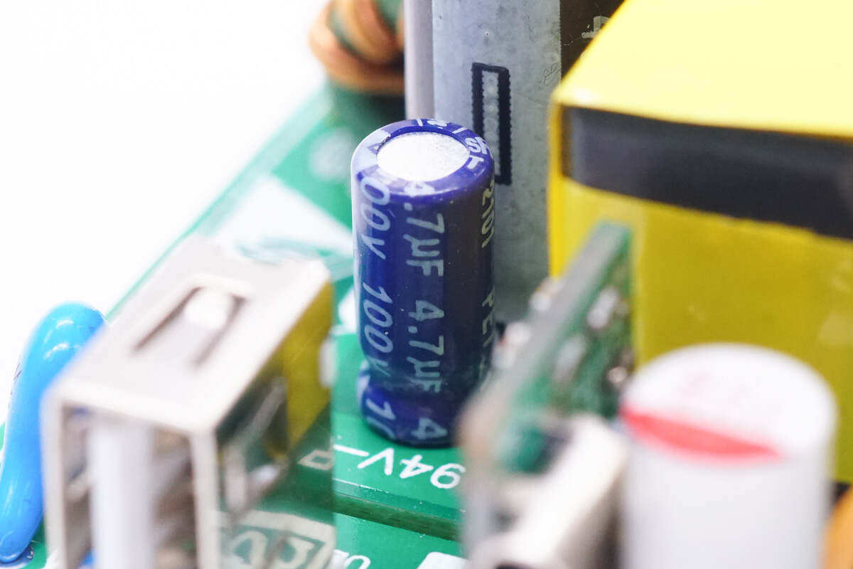
The specification of three high-voltage filter capacitors is 22 μ F400V.
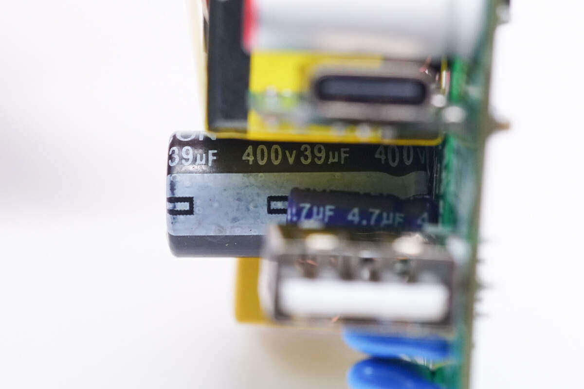
The other high-voltage filter capacitor is 400V39 μ F.
The differential inductance is wrapped with heat shrinkable tube for insulation.
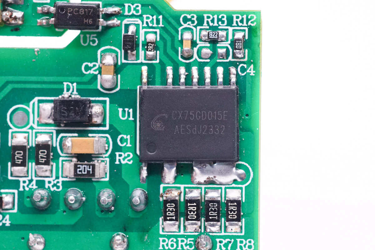
The GaN sealing chip is from Chengxin Micro, model CX75GD015E, which is internally integrated with 750V withstand voltage, 150m Ω conductive GaN switch tube, and supports 65W output power.The switching frequency of the chip is up to 200KHz, which supports full range quasi resonant mode operation. When light load is applied, it enters burst mode to improve efficiency, and there is no audio noise in the full operating range.
Chengxin Micro CX75GD015E supports 9-40V working voltage. The chip has built-in input overvoltage/undervoltage protection, built-in output overvoltage protection, built-in power supply overvoltage/undervoltage protection, built-in overpower and short circuit protection, built-in pin open circuit and short circuit protection, and built-in overheat protection function.
Chengxin Micro CX75GD015E adopts ESOP-10W packaging, which has excellent heat dissipation performance. By integrating GaN switch tubes and controllers, it improves the conversion efficiency, power density, reliability and switching frequency, reduces the impact of parasitic parameters on the system, reduces the number of components, and simplifies the design of fast charging power supply.
Data information of Chengxin Micro CX75GD015E.
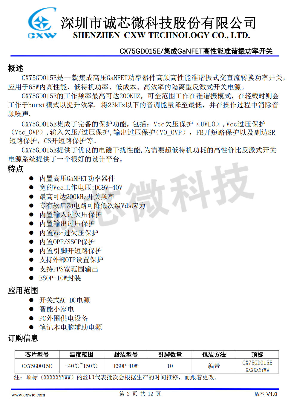
The filter capacitor specification for GaN sealing chip power supply is 4.7 μ F100V.
The other side of the mainboard is equipped with a transformer.
The transformer core is wound with tape for insulation, and the secondary is wound with multi-layer insulated wires.
PC817 optocoupler is used for output voltage feedback regulation.
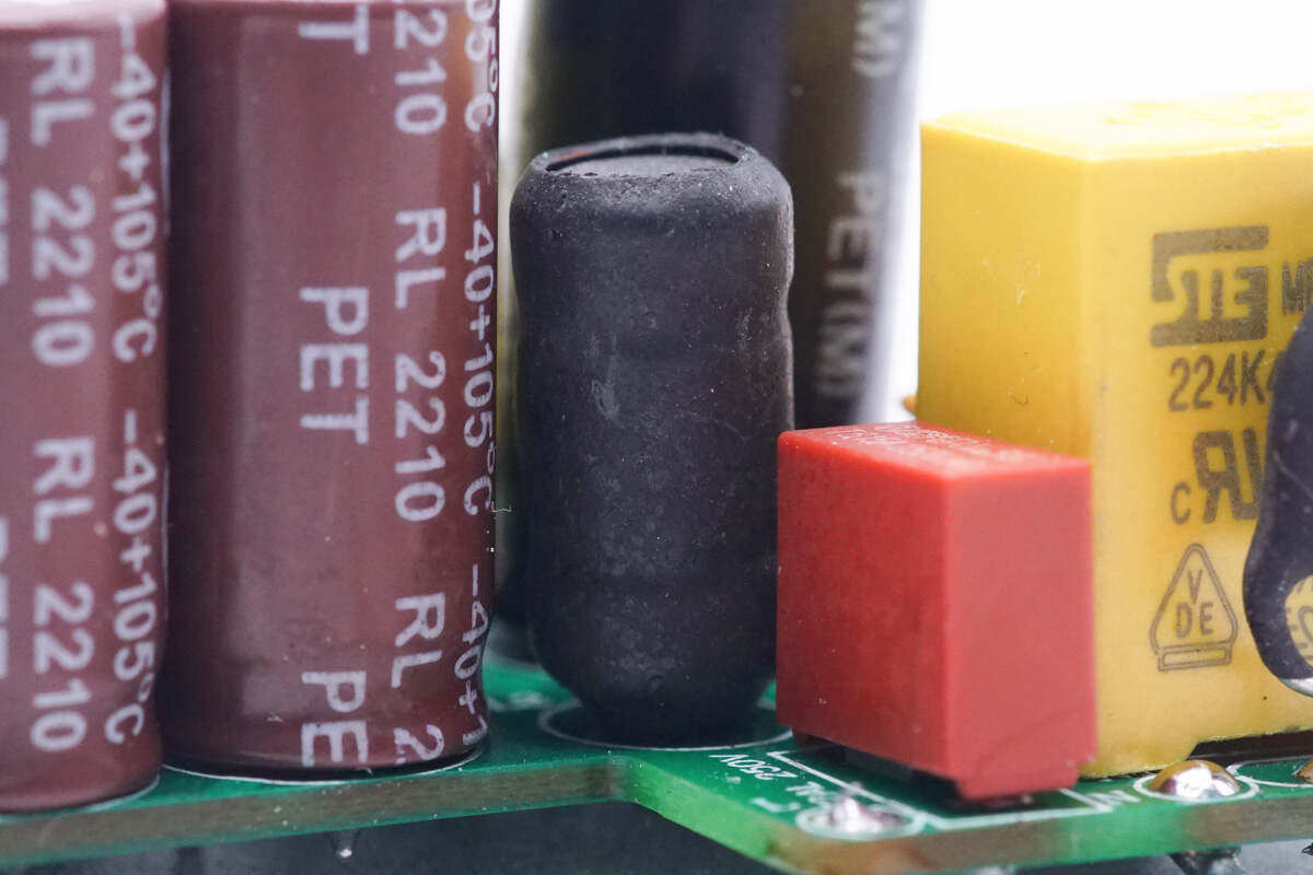
Close up of two blue Y capacitors.
The synchronous rectifier chip is from Chengxin Micro, model CX7539F. It is a high-performance synchronous rectifier chip at the secondary side of the switching power supply. It can easily meet the level 6 energy efficiency in the switching power supply, and is an ideal alternative for Schottky.The CX7539F supports a maximum switching frequency of 150KHz, built-in 10m Ω low resistance NMOS tube, and supports 5A output current.
Chengxin micro CX7539F synchronous rectification chip supports CCM/QR/DCM working mode. The chip adopts unique VDD power supply technology, has 4.5A driving current, uses low resistance MOS tube, has extremely low conduction voltage drop, generates much less heat than Schottky diode, greatly reduces temperature and improves conversion efficiency.
Chengxin Micro CX7539F information.
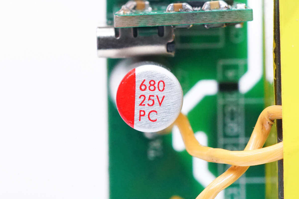
Output configuration1A1CDual output interface, there is also an output filter solid state capacitor on the right board of the USB-C bus base.
The specification of output filter solid capacitance is 680 μ F25V.
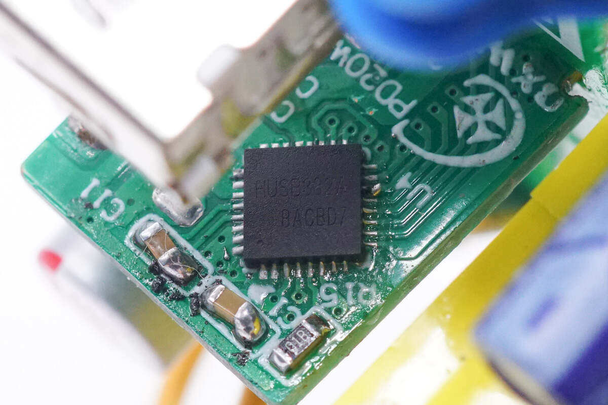
The protocol chip is from Huinengtai, model HUSB382A. It is a protocol chip supporting USB-C and USB-A ports. The chip is internally integrated with VBUS switch tubes for output control of two interfaces, further simplifying peripheral components.It supports five FPDOs and two programmable APDOs. It also supports common fast charging protocols, integrates Chip Link technology, and supports multi chip collaboration.
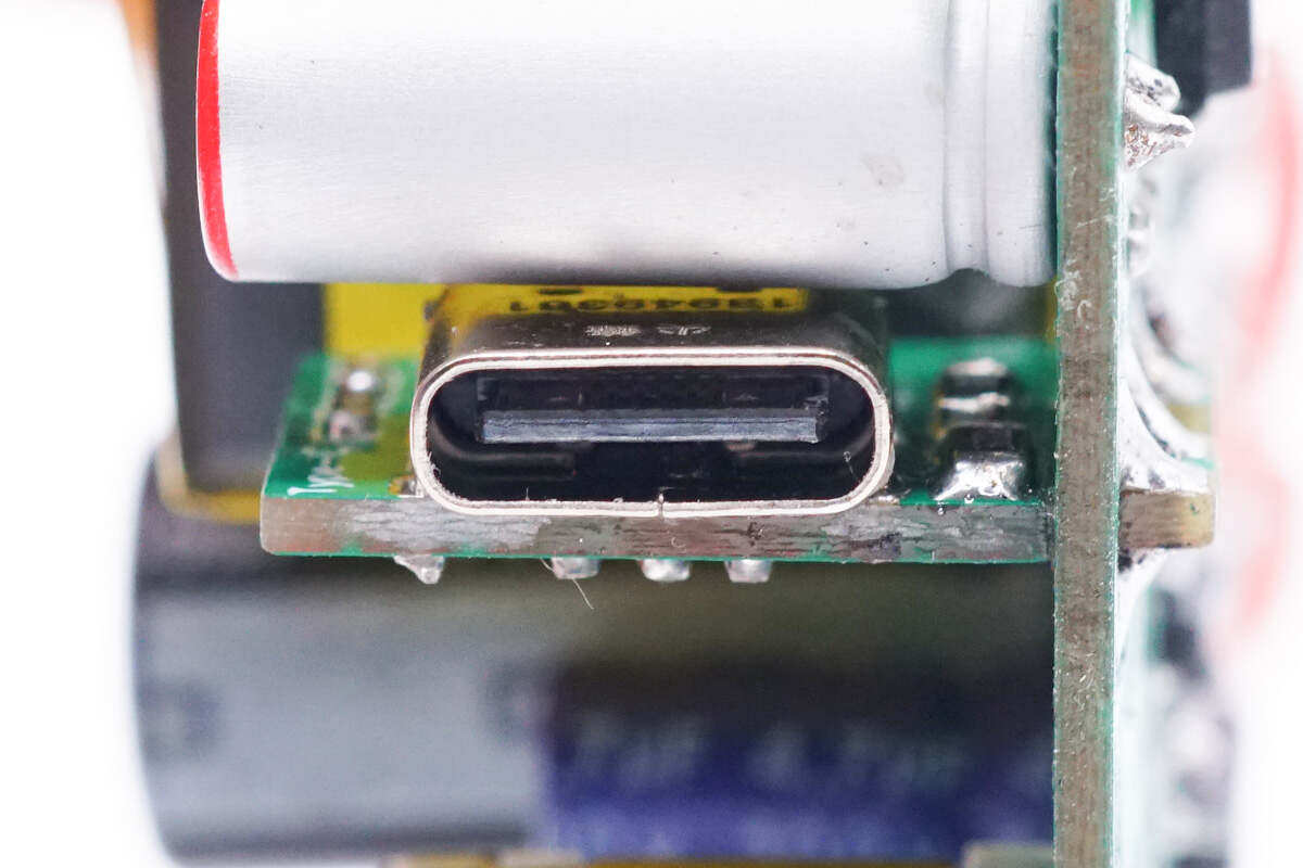
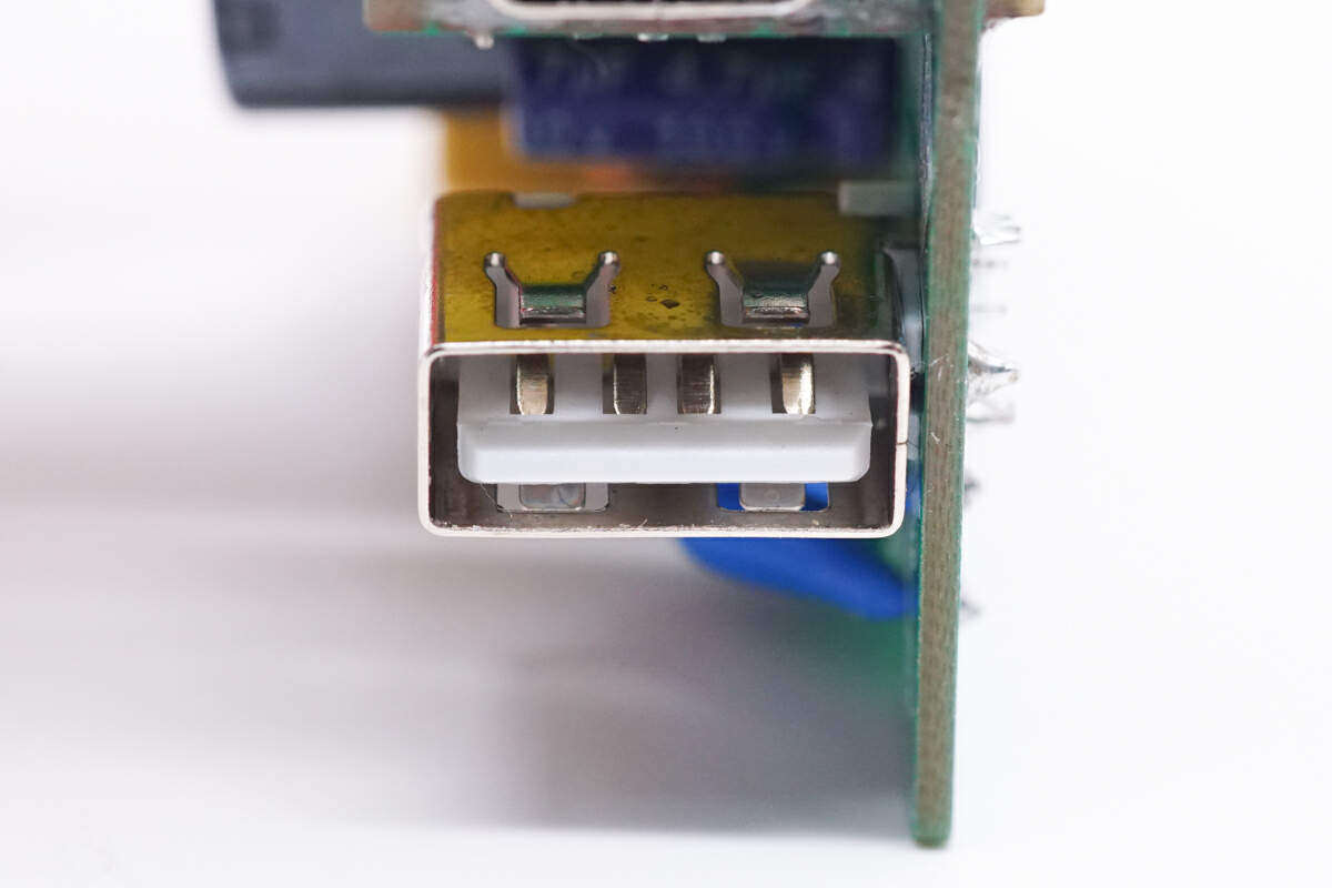
The USB-C mother seat is fixed by via welding, and the black rubber core does not expose copper.
USB-A mother seat adopts white rubber core and is fixed by via welding.
Summary of charging head network
Through the analysis of the reference design of Chengxin Micro 65W GaN fast charge, it is found that this reference design uses two highly integrated chips, which greatly simplifies the circuit design of the charger, reduces the number of components, and reduces the difficulty of debugging.Among them, the CX75GD015E GaN sealing chip is internally integrated with a 750V withstand voltage, 150m Ω conductive GaN switch tube, which is packaged with ESOP-10W and has excellent heat dissipation performance, supporting 65W fast charging applications.
The synchronous rectification chip adopts CX7539F, and the chip is encapsulated with DT-SOP7. A synchronous rectification tube with 10m Ω resistance is built in, which supports 5A output current and meets the requirements of fast charging with large current.Both chips are integrated with complete and comprehensive protection functions internally to meet the requirements of low standby power consumption and high conversion efficiency. They are very suitable for high-performance GaN PD fast charging, notebook power adapter, fast charging plug-in and other applications.
Chengxin micro varietySealed gallium nitrideThe scheme is launched, covering 20W, 30W, 45W, 65W, 100W and other multi power bands.OneSealed gallium nitrideThe chip can easily replace the function of two or three chips at the primary side. Through the highly integrated sealing chip, a simple and efficient GaN charger can be designed, which can effectively simplify the design and production process of the charger, thus helping industry customers quickly seize the market.